- 您现在的位置:买卖IC网 > PDF目录17059 > AD9148-M5375-EBZ (Analog Devices Inc)BOARD EVAL FOR AD9149, ADL5375 PDF资料下载
参数资料
| 型号: | AD9148-M5375-EBZ |
| 厂商: | Analog Devices Inc |
| 文件页数: | 35/72页 |
| 文件大小: | 0K |
| 描述: | BOARD EVAL FOR AD9149, ADL5375 |
| 设计资源: | AD9148-M5375-EBZ Schematic AD9148-M5375-EBZ BOM AD9148-M5375-EBZ Gerber Files |
| 标准包装: | 1 |
| 系列: | * |
第1页第2页第3页第4页第5页第6页第7页第8页第9页第10页第11页第12页第13页第14页第15页第16页第17页第18页第19页第20页第21页第22页第23页第24页第25页第26页第27页第28页第29页第30页第31页第32页第33页第34页当前第35页第36页第37页第38页第39页第40页第41页第42页第43页第44页第45页第46页第47页第48页第49页第50页第51页第52页第53页第54页第55页第56页第57页第58页第59页第60页第61页第62页第63页第64页第65页第66页第67页第68页第69页第70页第71页第72页
AD9148
Data Sheet
Rev. B | Page 40 of 72
INPUT DATA PORTS
The AD9148 can operate in three data input modes: dual-port
mode, single-port mode, and byte mode. In dual-port mode,
DAC 1 and DAC 2 receive data from Port A, and DAC 3 and
DAC 4 receive data from Port B. In single-port mode, all four
DACs receive data from Port A. In byte mode, all four DACs
receive data from Port A, but the port is split into two 8-bit wide
buses. In all modes, the data input timing is relative to a DCI signal
provided with the data.
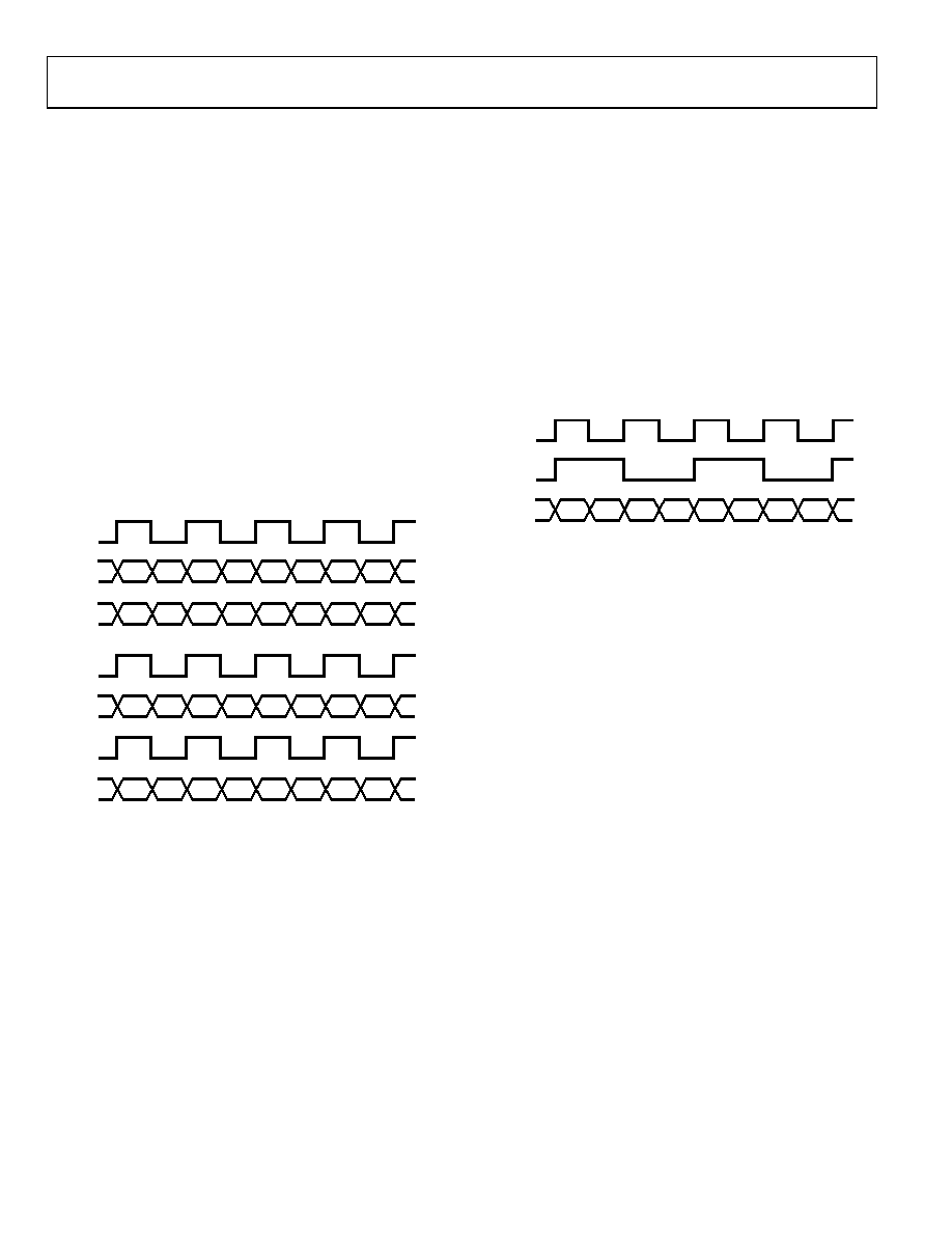
DUAL-PORT MODE
In dual-port mode, the DCI signal indicates to which DAC the
data is intended. On the rising edge of DCI, data is latched into
DAC 1 and DAC 3. On the falling edge of DCI, data is latched
into DAC 2 and DAC 4. This pattern repeats continuously.
There is a SPI programmable option (Register 0x14[6]) to provide
one DCI for both input ports or two DCIs, where each DCI is
associated with one input port. Two DCIs are useful when the
data for each port is coming from a different data source. These
cases are illustrated in Figure 45 and Figure 46.
DCIA
A[15:0]
DAC1
DAC2
DAC1
DAC2
DAC1
DAC2
DAC1
DAC2
DAC3
DAC4
DAC3
DAC4
DAC3
DAC4
DAC3
DAC4
B[15:0]
08910-
045
Figure 45. Timing Diagram for Dual-Port Mode, One DCI
DCIA
A[15:0]
DAC1
DAC2
DAC1
DAC2
DAC1
DAC2
DAC1
DAC2
DAC3
DAC4
DAC3
DAC4
DAC3
DAC4
DAC3
DAC4
B[15:0]
DCIB
08910-
046
Figure 46. Timing Diagram for Dual-Port Mode, Two DCI
Each data sample, by default, is expected to be formatted as an
MSB sent to Bit 15 and an LSB sent to Bit 0 for each port. The
AD9148 contains an option to swap the bus (Register 0x03[4]).
When this bus swap bit is set, the MSB should be sent to Bit 0,
and the LSB should be sent to Bit 15 for each port.
SINGLE-PORT MODE
In single-port mode, a FRAME signal must be provided along
with the DCI signal and the data. The FRAME signal indicates
to which DAC the data is intended. When FRAME goes high,
the first data-word goes to DAC 1, and the second data-word
goes to DAC 2. When FRAME goes low, the first data-word
goes to DAC 3, and the second data-word goes to DAC 4.
This pattern repeats continuously as illustrated in Figure 47.
FRAMEA
A[15:0]
DAC1
DAC2
DAC3
DAC4
DAC1
DAC2
DAC3
DAC4
DCIA
08910-
047
Figure 47. Timing Diagram for Single-Port Mode
Each data sample, by default, is expected to be formatted as an MSB
sent to Bit 15 and an LSB sent to Bit 0. When the bus swap bit is
set (Register 0x03[4]), the MSB should be sent to Bit 0, and the
LSB should be sent to Bit 15 for each port.
The FRAME signal is sampled with the same internal signal as
the data and has the same set-up and hold timing relative to DCI. If
desired, only the first FRAME pulse needs to be generated. This
initializes the internal clock phases inside the device, and data
latches just as if the periodic FRAME signal were sent.
相关PDF资料 |
PDF描述 |
|---|---|
| UPB2G181MRD6 | CAP ALUM 180UF 400V 20% RADIAL |
| VE-B64-EY | CONVERTER MOD DC/DC 48V 50W |
| AD9148-M5372-EBZ | BOARD EVAL FOR AD9149, ADL5372 |
| AD9737A-EBZ | BOARD EVAL FOR AD9737A |
| MIC2026-1YM | IC DISTRIBUTION SW DUAL 8-SOIC |
相关代理商/技术参数 |
参数描述 |
|---|---|
| AD9152BCPZ | 功能描述:16 Bit Digital to Analog Converter 2 56-LFCSP-WQ (8x8) 制造商:analog devices inc. 系列:TxDAC+? 包装:托盘 零件状态:有效 位数:16 数模转换器数:2 建立时间:- 输出类型:Current - Unbuffered 差分输出:是 数据接口:JESD204B 参考类型:内部 电压 - 电源,模拟:3.13 V ~ 3.47 V 电压 - 电源,数字:1.14 V ~ 1.26 V INL/DNL(LSB):±10,±5 架构:电流源 工作温度:-40°C ~ 85°C 封装/外壳:56-WFQFN 裸焊盘,CSP 供应商器件封装:56-LFCSP-WQ(8x8) 标准包装:1 |
| AD9152BCPZRL | 功能描述:16 Bit Digital to Analog Converter 2 56-LFCSP-WQ (8x8) 制造商:analog devices inc. 系列:TxDAC+? 包装:带卷(TR) 零件状态:有效 位数:16 数模转换器数:2 建立时间:- 输出类型:Current - Unbuffered 差分输出:是 数据接口:JESD204B 参考类型:内部 电压 - 电源,模拟:3.13 V ~ 3.47 V 电压 - 电源,数字:1.14 V ~ 1.26 V INL/DNL(LSB):±10,±5 架构:电流源 工作温度:-40°C ~ 85°C 封装/外壳:56-WFQFN 裸焊盘,CSP 供应商器件封装:56-LFCSP-WQ(8x8) 标准包装:2,500 |
| AD9152-EBZ | 功能描述:AD9152 TxDAC+? Series 16 Bit 2.25G Samples Per Second Digital to Analog Converter (DAC) Evaluation Board 制造商:analog devices inc. 系列:TxDAC+? 零件状态:有效 DAC 数:2 位数:16 采样率(每秒):2.25G 数据接口:SPI 建立时间:- DAC 类型:电流 工作温度:-40°C ~ 85°C 所含物品:板,线缆 使用的 IC/零件:AD9152 标准包装:1 |
| AD9152-FMC-EBZ | 功能描述:AD9152 TxDAC+? Series 16 Bit 2.25G Samples Per Second Digital to Analog Converter (DAC) Evaluation Board 制造商:analog devices inc. 系列:TxDAC+? 零件状态:有效 DAC 数:2 位数:16 采样率(每秒):2.25G 数据接口:SPI 建立时间:- DAC 类型:电流 工作温度:-40°C ~ 85°C 所含物品:板,线缆 使用的 IC/零件:AD9152 标准包装:1 |
| AD9152-M6720-EBZ | 功能描述:AD9152 TxDAC+? Series 16 Bit 2.25G Samples Per Second Digital to Analog Converter (DAC) Evaluation Board 制造商:analog devices inc. 系列:TxDAC+? 零件状态:有效 DAC 数:2 位数:16 采样率(每秒):2.25G 数据接口:SPI 建立时间:- DAC 类型:电流 工作温度:-40°C ~ 85°C 所含物品:板 使用的 IC/零件:AD9152 标准包装:1 |
发布紧急采购,3分钟左右您将得到回复。