- 您现在的位置:买卖IC网 > PDF目录17059 > AD9148-M5375-EBZ (Analog Devices Inc)BOARD EVAL FOR AD9149, ADL5375 PDF资料下载
参数资料
| 型号: | AD9148-M5375-EBZ |
| 厂商: | Analog Devices Inc |
| 文件页数: | 42/72页 |
| 文件大小: | 0K |
| 描述: | BOARD EVAL FOR AD9149, ADL5375 |
| 设计资源: | AD9148-M5375-EBZ Schematic AD9148-M5375-EBZ BOM AD9148-M5375-EBZ Gerber Files |
| 标准包装: | 1 |
| 系列: | * |
第1页第2页第3页第4页第5页第6页第7页第8页第9页第10页第11页第12页第13页第14页第15页第16页第17页第18页第19页第20页第21页第22页第23页第24页第25页第26页第27页第28页第29页第30页第31页第32页第33页第34页第35页第36页第37页第38页第39页第40页第41页当前第42页第43页第44页第45页第46页第47页第48页第49页第50页第51页第52页第53页第54页第55页第56页第57页第58页第59页第60页第61页第62页第63页第64页第65页第66页第67页第68页第69页第70页第71页第72页
Data Sheet
AD9148
Rev. B | Page 47 of 72
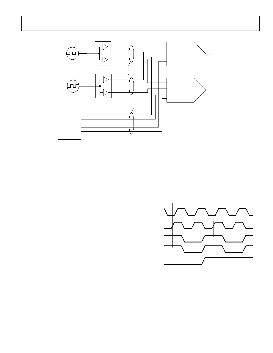
SAMPLE RATE CLOCK
FPGA
LOW SKEW
CLOCK DRIVER
LOW SKEW
CLOCK DRIVER
MATCHED
LENGTH TRACES
CLK
FRAME
DCI
OUT1
OUT2
SYNC CLOCK
REFCLK/SYNC
CLK
FRAME
DCI
REFCLK/SYNC
MATCHED
LENGTH TRACES
08910-
054
Figure 55. Typical Circuit Diagram for Synchronizing Devices to a System Clock
SYNCHRONIZATION WITH DIRECT CLOCKING
When directly sourcing the DAC sample rate clock to CLK, a
separate REFCLK/SYNC input signal is required for synchronization.
To synchronize devices, the CLK signals and the REFCLK/SYNC
signals must be distributed with low skew to all of the devices
being synchronized. This configuration is shown below in
Data Rate Mode Synchronization
The following procedure outlines the steps required to synchronize
multiple devices in data rate mode. The procedure assumes that
the CLK and REFCLK/SYNC signals are applied to all of the
devices. Each individual device must follow the procedure.
The procedure for data rate synchronization when directly
sourcing the DAC sampling clock follows:
1. Configure for data rate, periodic synchronization by
writing 0xC0 to the sync control register (Register 0x10).
Additional synchronization options are available (see the
2. Poll the sync locked bit (Bit 6, Register 0x12) to verify that
the device is back-end synchronized. A high level on this
bit indicates that the clocks are running with a constant
and known phase relative to the sync signal.
3. Reset the FIFO by strobing the FRAME signal for at least the
time interval needed to load complete data to the four DACs
Resetting the FIFO ensures that the correct data is being
read from the FIFO of each of the devices simultaneously.
This completes the synchronization procedure, and at this
stage, all devices should be synchronized.
To ensure that each of the DACs are updated with the correct data
on the same DACCLK edge, two timing relationships must be
met on each DAC. DCI (and data) must meet the setup and hold
times with respect to the rising edge of CLK, and REFCLK/SYNC
must also meet the setup and hold time with respect to the
rising edge of CLK. When resetting the FIFO, the FRAME
signal must be held high for at least the time interval needed to
load complete data to the four DACs (one DCI period for dual-
port mode and two DCI periods for single-port or byte mode).
When these conditions are met, the outputs of the DACs will be
updated within tSKEW + tOUTDLY nanoseconds of each other. A timing
diagram that illustrates the timing requirements of the input
signals is shown in Figure 56.
CLK(1)
CLK(2)
SYNC(2)
FRAME(2)
DCI(2)
tSKEW
tH_DCI
tSU_DCI
tH_SYNC
tSU_SYNC
08910-
055
Figure 56. Synchronization Signal Timing Requirements in Data Rate Mode,
2× Interpolation
Figure 56 shows the synchronization signal timing with 2×
interpolation, so that fDCI = × fCLK. The REFCLK/SYNC input
is shown equal to the DCI rate. The maximum frequency at which
the device can be resynchronized in data rate mode can be
expressed as
N
DATA
SYNC
f
2
=
for any positive integer, N.
相关PDF资料 |
PDF描述 |
|---|---|
| UPB2G181MRD6 | CAP ALUM 180UF 400V 20% RADIAL |
| VE-B64-EY | CONVERTER MOD DC/DC 48V 50W |
| AD9148-M5372-EBZ | BOARD EVAL FOR AD9149, ADL5372 |
| AD9737A-EBZ | BOARD EVAL FOR AD9737A |
| MIC2026-1YM | IC DISTRIBUTION SW DUAL 8-SOIC |
相关代理商/技术参数 |
参数描述 |
|---|---|
| AD9152BCPZ | 功能描述:16 Bit Digital to Analog Converter 2 56-LFCSP-WQ (8x8) 制造商:analog devices inc. 系列:TxDAC+? 包装:托盘 零件状态:有效 位数:16 数模转换器数:2 建立时间:- 输出类型:Current - Unbuffered 差分输出:是 数据接口:JESD204B 参考类型:内部 电压 - 电源,模拟:3.13 V ~ 3.47 V 电压 - 电源,数字:1.14 V ~ 1.26 V INL/DNL(LSB):±10,±5 架构:电流源 工作温度:-40°C ~ 85°C 封装/外壳:56-WFQFN 裸焊盘,CSP 供应商器件封装:56-LFCSP-WQ(8x8) 标准包装:1 |
| AD9152BCPZRL | 功能描述:16 Bit Digital to Analog Converter 2 56-LFCSP-WQ (8x8) 制造商:analog devices inc. 系列:TxDAC+? 包装:带卷(TR) 零件状态:有效 位数:16 数模转换器数:2 建立时间:- 输出类型:Current - Unbuffered 差分输出:是 数据接口:JESD204B 参考类型:内部 电压 - 电源,模拟:3.13 V ~ 3.47 V 电压 - 电源,数字:1.14 V ~ 1.26 V INL/DNL(LSB):±10,±5 架构:电流源 工作温度:-40°C ~ 85°C 封装/外壳:56-WFQFN 裸焊盘,CSP 供应商器件封装:56-LFCSP-WQ(8x8) 标准包装:2,500 |
| AD9152-EBZ | 功能描述:AD9152 TxDAC+? Series 16 Bit 2.25G Samples Per Second Digital to Analog Converter (DAC) Evaluation Board 制造商:analog devices inc. 系列:TxDAC+? 零件状态:有效 DAC 数:2 位数:16 采样率(每秒):2.25G 数据接口:SPI 建立时间:- DAC 类型:电流 工作温度:-40°C ~ 85°C 所含物品:板,线缆 使用的 IC/零件:AD9152 标准包装:1 |
| AD9152-FMC-EBZ | 功能描述:AD9152 TxDAC+? Series 16 Bit 2.25G Samples Per Second Digital to Analog Converter (DAC) Evaluation Board 制造商:analog devices inc. 系列:TxDAC+? 零件状态:有效 DAC 数:2 位数:16 采样率(每秒):2.25G 数据接口:SPI 建立时间:- DAC 类型:电流 工作温度:-40°C ~ 85°C 所含物品:板,线缆 使用的 IC/零件:AD9152 标准包装:1 |
| AD9152-M6720-EBZ | 功能描述:AD9152 TxDAC+? Series 16 Bit 2.25G Samples Per Second Digital to Analog Converter (DAC) Evaluation Board 制造商:analog devices inc. 系列:TxDAC+? 零件状态:有效 DAC 数:2 位数:16 采样率(每秒):2.25G 数据接口:SPI 建立时间:- DAC 类型:电流 工作温度:-40°C ~ 85°C 所含物品:板 使用的 IC/零件:AD9152 标准包装:1 |
发布紧急采购,3分钟左右您将得到回复。