参数资料
| 型号: | AD9148BBPZ |
| 厂商: | Analog Devices Inc |
| 文件页数: | 43/72页 |
| 文件大小: | 0K |
| 描述: | IC DAC 16BIT SPI/SRL 196BGA |
| 标准包装: | 1 |
| 系列: | TxDAC+® |
| 设置时间: | 20ns |
| 位数: | 16 |
| 数据接口: | 串行,SPI? |
| 转换器数目: | 4 |
| 电压电源: | 单电源 |
| 功率耗散(最大): | 2.67W |
| 工作温度: | -40°C ~ 85°C |
| 安装类型: | 表面贴装 |
| 封装/外壳: | 196-LFBGA 裸露焊盘 |
| 供应商设备封装: | 196-BGA |
| 包装: | 托盘 |
| 输出数目和类型: | 4 电流,单极 |
| 采样率(每秒): | 1G |
第1页第2页第3页第4页第5页第6页第7页第8页第9页第10页第11页第12页第13页第14页第15页第16页第17页第18页第19页第20页第21页第22页第23页第24页第25页第26页第27页第28页第29页第30页第31页第32页第33页第34页第35页第36页第37页第38页第39页第40页第41页第42页当前第43页第44页第45页第46页第47页第48页第49页第50页第51页第52页第53页第54页第55页第56页第57页第58页第59页第60页第61页第62页第63页第64页第65页第66页第67页第68页第69页第70页第71页第72页
AD9148
Data Sheet
Rev. B | Page 48 of 72
Generally, for values of N equal to or greater than 3, the FIFO
rate synchronization mode is chosen.
FIFO Rate Mode Synchronization
The following procedure outlines the steps required to synchronize
multiple devices in FIFO rate mode. The procedure assumes
that the CLK and REFCLK/SYNC signals are applied to all of the
devices. Each individual device must follow the procedure.
The procedure for FIFO rate synchronization when directly
sourcing the DAC sampling clock follows:
1. Configure for FIFO rate, periodic synchronization by writing
0x80 to the sync control register (Register 0x10). Additional
synchronization options are available and are described in
the Additional Synchronization Features section.
2. Poll the sync locked bit (Bit 6, Register 0x12) to verify that
the device is back-end synchronized. A high level on this
bit indicates that the clocks are running with a constant
and known phase relative to the sync signal.
3. Reset the FIFO by strobing the FRAME signal high for at
least the time interval needed to load complete data to the
four DACs. Resetting the FIFO ensures that the correct
data is being read from the FIFO of each of the devices
simultaneously. This completes the synchronization
procedure, and at this stage, all devices should be
synchronized.
To ensure that each of the DACs is updated with the correct
data on the same DACCLK edge, two timing relationships must
be met on each DAC. DCI (and data) must meet the setup and
hold times with respect to the rising edge of CLK, and REFCLK/
SYNC must also meet the setup and hold time with respect to
the rising edge of CLK. When resetting the FIFO, the FRAME
signal must be held high for at least the time interval needed to
load complete data to the four DACs (one DCI period for dual-
port mode, and two DCI periods for single-port or byte mode).
When these conditions are met, the outputs of the DACs will be
updated within tSKEW + tOUTDLY nanoseconds of each other. A
timing diagram that illustrates the timing requirements of the
input signals is shown in Figure 57.
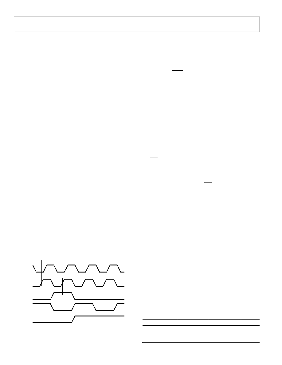
CLK(1)
CLK(2)
SYNC(2)
FRAME(2)
DCI(2)
tSKEW
tH_SYNC
tSU_SYNC
08910-
056
Figure 57. Synchronization Signal Timing Requirements in FIFO Rate Mode,
2× Interpolation
Figure 57 shows the synchronization signal timing with 2×
interpolation, so that fDCI = × fCLK. The REFCLK/SYNC input
is shown equal to the FIFO rate. The maximum frequency at which
the device can be resynchronized in FIFO rate mode can be
expressed as
N
DATA
SYNC
f
2
8×
=
for any positive integer, N.
ADDITIONAL SYNCHRONIZATION FEATURES
The synchronization logic incorporates additional features that
provide means for querying the status of the synchronization
and for improving the robustness of the synchronization. For
more information on these features, see the Sync Status Bits
section and the Timing Optimization section.
Sync Status Bits
When the sync locked bit (Bit 6, Register 0x12) is set, it indicates
that the synchronization logic has reached alignment. This is
determined when the clock generation state machine phase is
constant. This takes between (11 + Averaging) × 64 and (11 +
Averaging) × 128 DACCLK cycles. This bit may optionally trigger
an IRQ, as described in the Interrupt Request Operation section.
When the sync lost bit (Bit 7, Register 0x12) is set, it indicates that a
previously synchronized device has lost alignment. This bit is
latched and remains set until cleared by overwriting the register.
This bit may optionally trigger an IRQ as described in the
Timing Optimization
The REFCLK/SYNC signal is sampled by a version of the
DACCLK. If sampling errors are detected, the opposite sampling
edge can be selected to improve the sampling point. The sampling
edge can be selected by setting Bit 3, Register 0x10 (1 = rising
and 0 = falling).
The synchronization logic resynchronizes when a phase change
between the REFCLK/SYNC signal and the state of the clock
generation state machine exceeds a threshold. To mitigate the
effects of jitter and prevent erroneous resynchronizations, the
relative phase can be averaged. The amount of averaging is set
by the sync averaging bits (Bits[2:0], Register 0x10) and can be
set from 1 to 128. The higher the number of averages, the more
slowly the device recognizes and resynchronizes to a legitimate
phase correction. Generally, the averaging should be made as
large as possible while still meeting the allotted resynchronization
time interval.
Additional information on synchronization can be found in the
AN-1093 Application Note, Synchronization of Multiple AD9122
TxDAC+ Converters.
Table 15. Synchronization Setup and Hold Times
Parameter
Min
Max
Unit
tSKEW
tDACCLK/2
+tDACCLK/2
ps
tSU_SYNC
100
ps
tH_SYNC
+400
ps
相关PDF资料 |
PDF描述 |
|---|---|
| MS27473T10B98PBLC | CONN HSG PLUG 6POS STRGHT PINS |
| LTC2758ACLX#PBF | IC DAC 18BIT SPI/SRL 48-LQFP |
| MS27468T15B19PLC | CONN HSG RCPT 19POS JAMNUT PINS |
| V24B5M200BF2 | CONVERTER MOD DC/DC 5V 200W |
| MS27656T23B35B | CONN HSG RCPT 100POS WALL MT SCK |
相关代理商/技术参数 |
参数描述 |
|---|---|
| AD9148BBPZRL | 功能描述:IC DAC 16BIT SPI/SRL 196BGA RoHS:是 类别:集成电路 (IC) >> 数据采集 - 数模转换器 系列:TxDAC+® 产品培训模块:Lead (SnPb) Finish for COTS Obsolescence Mitigation Program 标准包装:1,000 系列:- 设置时间:1µs 位数:8 数据接口:串行 转换器数目:8 电压电源:双 ± 功率耗散(最大):941mW 工作温度:0°C ~ 70°C 安装类型:表面贴装 封装/外壳:24-SOIC(0.295",7.50mm 宽) 供应商设备封装:24-SOIC W 包装:带卷 (TR) 输出数目和类型:8 电压,单极 采样率(每秒):* |
| AD9148BPCZ | 制造商:AD 制造商全称:Analog Devices 功能描述:Quad 16-Bit,1 GSPS, TxDAC+ Digital-to-Analog Converter |
| AD9148BPCZRL | 制造商:AD 制造商全称:Analog Devices 功能描述:Quad 16-Bit,1 GSPS, TxDAC+ Digital-to-Analog Converter |
| AD9148-EBZ | 功能描述:BOARD EVALUATION FOR AD9148 RoHS:是 类别:编程器,开发系统 >> 评估板 - 数模转换器 (DAC) 系列:TxDAC+® 产品培训模块:Lead (SnPb) Finish for COTS Obsolescence Mitigation Program 标准包装:1 系列:- DAC 的数量:4 位数:12 采样率(每秒):- 数据接口:串行,SPI? 设置时间:3µs DAC 型:电流/电压 工作温度:-40°C ~ 85°C 已供物品:板 已用 IC / 零件:MAX5581 |
| AD9148-M5372-EBZ | 功能描述:BOARD EVAL FOR AD9149, ADL5372 RoHS:是 类别:编程器,开发系统 >> 评估板 - 数模转换器 (DAC) 系列:* 产品培训模块:Lead (SnPb) Finish for COTS Obsolescence Mitigation Program 标准包装:1 系列:- DAC 的数量:4 位数:12 采样率(每秒):- 数据接口:串行,SPI? 设置时间:3µs DAC 型:电流/电压 工作温度:-40°C ~ 85°C 已供物品:板 已用 IC / 零件:MAX5581 |
发布紧急采购,3分钟左右您将得到回复。