参数资料
| 型号: | AD9148BBPZ |
| 厂商: | Analog Devices Inc |
| 文件页数: | 58/72页 |
| 文件大小: | 0K |
| 描述: | IC DAC 16BIT SPI/SRL 196BGA |
| 标准包装: | 1 |
| 系列: | TxDAC+® |
| 设置时间: | 20ns |
| 位数: | 16 |
| 数据接口: | 串行,SPI? |
| 转换器数目: | 4 |
| 电压电源: | 单电源 |
| 功率耗散(最大): | 2.67W |
| 工作温度: | -40°C ~ 85°C |
| 安装类型: | 表面贴装 |
| 封装/外壳: | 196-LFBGA 裸露焊盘 |
| 供应商设备封装: | 196-BGA |
| 包装: | 托盘 |
| 输出数目和类型: | 4 电流,单极 |
| 采样率(每秒): | 1G |
第1页第2页第3页第4页第5页第6页第7页第8页第9页第10页第11页第12页第13页第14页第15页第16页第17页第18页第19页第20页第21页第22页第23页第24页第25页第26页第27页第28页第29页第30页第31页第32页第33页第34页第35页第36页第37页第38页第39页第40页第41页第42页第43页第44页第45页第46页第47页第48页第49页第50页第51页第52页第53页第54页第55页第56页第57页当前第58页第59页第60页第61页第62页第63页第64页第65页第66页第67页第68页第69页第70页第71页第72页
Data Sheet
AD9148
Rev. B | Page 61 of 72
In addition, the P or N output can act as a current source or a
current sink. When sourcing current, the output compliance
voltage is 0 V to 1.6 V. When sinking current, the output compliance
voltage is 0.8 V to 1.6 V. The auxiliary DAC current direction is
programmable via Bit 6, Register 0x33 and Bit 6, Register 0x37
(DAC SPI select is 0 to control AUX1 and AUX2, and DAC SPI
select is 1 to control AUX3 and AUX4). The choice of sinking or
sourcing should be made at circuit design time. There is no
advantage to switching between sourcing and sinking current
after the circuit is in place.
These auxiliary DACs can be used for local oscillator (LO)
cancellation when the DAC output is followed by a quadrature
modulator. More information and example application circuits
are given in the Interfacing to Modulators section.
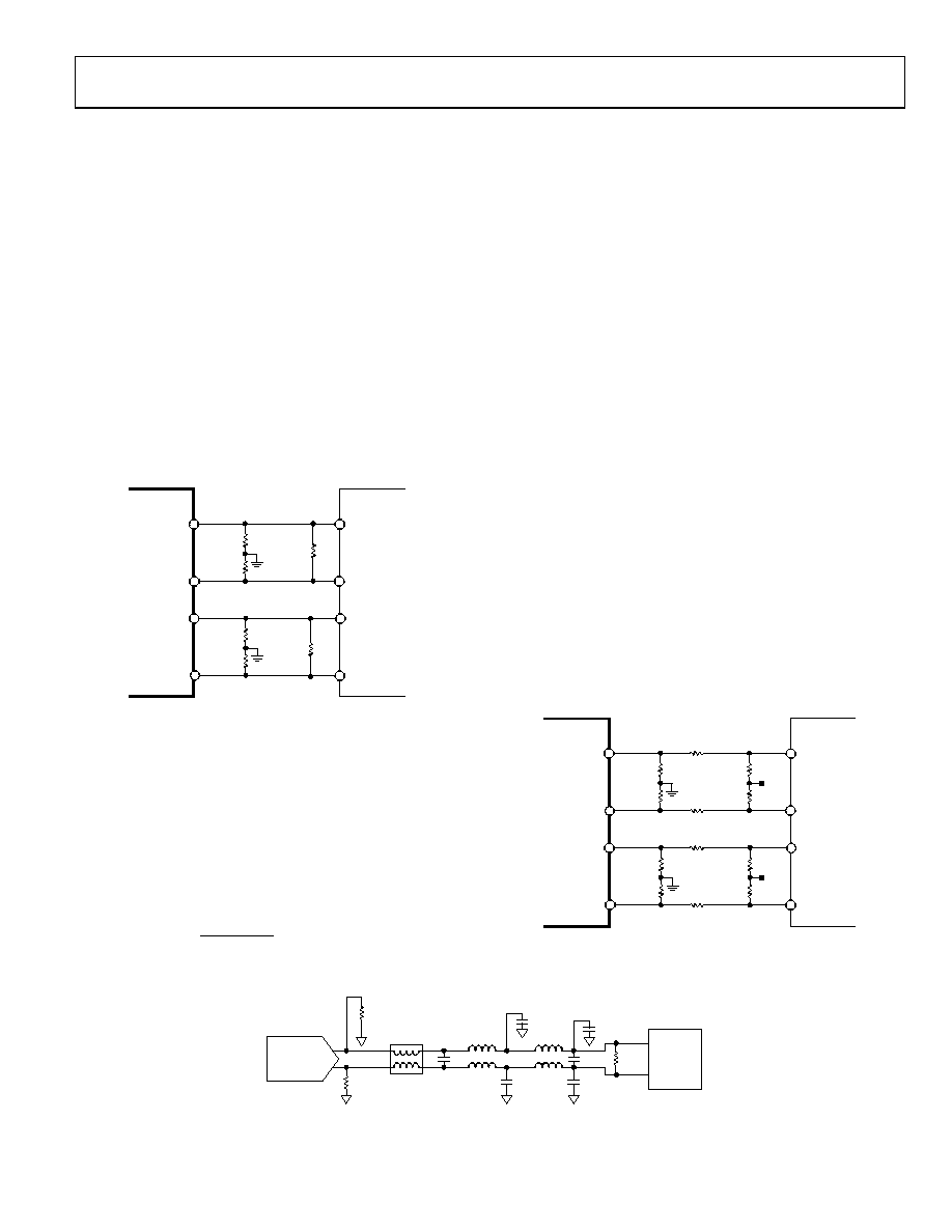
INTERFACING TO MODULATORS
The AD9148 interfaces to the ADL537x family with a minimal
number of components. An example of the recommended
interface circuitry is shown in Figure 81.
RBIP
50
RBIN
50
IBBN
IBBP
AD9148
ADL537x
RBQN
50
RBQP
50
RLI
100
RLQ
100
IOUT1_N
IOUT1_P
IOUT2_P
IOUT2_N
QBBP
QBBN
08910-
079
Figure 81. Typical Interface Circuitry Between the AD9148 and ADL537x
Family of Modulators
The baseband inputs of the ADL537x family require a dc bias
of 500 mV. The nominal midscale output current on each output
of the DAC is 10 mA (1/2 the full-scale current). Therefore, a
single 50 resistor to ground from each of the DAC outputs
results in the desired 500 mV dc common-mode bias for the
inputs to the ADL537x. The signal level can be reduced by the
addition of the load resistor in parallel with the modulator inputs
(RLI, RLQ). The peak-to-peak voltage swing of the transmitted
signal is
[
]
[
]
L
B
L
B
FS
SIGNAL
R
I
V
+
×
=
2
Baseband Filter Implementation
Most applications require a baseband anti-imaging filter between
the DAC and modulator to filter out Nyquist images and broadband
DAC noise. The filter can be inserted between the I-to-V resistors
at the DAC output and the signal level setting resistor across the
modulator input. Doing this establishes the input and output
impedances for the filter.
Figure 83 shows a fifth-order low-pass filter. A common-mode
choke is used between the I-to-V resistors and the remainder
of the filter. This removes the common-mode signal produced
by the DAC and prevents the common-mode signal from being
converted to a differential signal, which would appear as unwanted
spurious signals in the output spectrum. The common-mode
choke or balun may not be needed if the layout between the
DAC and IQ modulator is optimized and balanced. Splitting
the second filter capacitor into two and grounding the center
point creates a common-mode low-pass filter, providing additional
common-mode rejection of high frequency signals. A purely
differential filter passes common-mode signals.
Driving the ADL5375-15 with the AD9148
The ADL5375-15 requires a 1500 mV dc bias and therefore
requires a slightly more complex interface than most other
Analog Devices, Inc., modulators. It is necessary to level shift
the DAC output from a 500 mV dc bias to the 1500 mV dc bias
that the ADL5375-15 requires. Level shifting can be achieved
with a purely passive network, as shown in Figure 82. In this
network, the dc bias of the DAC remains at 500 mV, while the
input to the ADL5375-15 is 1500 mV. Note that this passive
level shifting network introduces approximately 2 dB of loss
in the ac signal.
IBBN
IBBP
AD9148
ADL5375-15
RBIP
45.3
RBIN
45.3
RBQN
45.3
RBQP
45.3
RLIP
3480
RLIN
3480
RLQN
3480
RLQP
3480
IOUT1_N
IOUT1_P
IOUT2_P
IOUT2_N
QBBP
QBBN
RSIN
1k
RSIP
1k
RSQN
1k
RSQP
1k
5V
08910-
081
Figure 82. Passive Level Shifting Network for Biasing
the ADL5375-15 from the AD9148
IDAC
OR
QDAC
50
MABACT0043
(OPTIONAL)
33nH
2pF
56nH
100
6pF
3pF
22pF
ADL537x
08910-
080
Figure 83. DAC Modulator Interface with Fifth-Order, Low Pass Filter
相关PDF资料 |
PDF描述 |
|---|---|
| MS27473T10B98PBLC | CONN HSG PLUG 6POS STRGHT PINS |
| LTC2758ACLX#PBF | IC DAC 18BIT SPI/SRL 48-LQFP |
| MS27468T15B19PLC | CONN HSG RCPT 19POS JAMNUT PINS |
| V24B5M200BF2 | CONVERTER MOD DC/DC 5V 200W |
| MS27656T23B35B | CONN HSG RCPT 100POS WALL MT SCK |
相关代理商/技术参数 |
参数描述 |
|---|---|
| AD9148BBPZRL | 功能描述:IC DAC 16BIT SPI/SRL 196BGA RoHS:是 类别:集成电路 (IC) >> 数据采集 - 数模转换器 系列:TxDAC+® 产品培训模块:Lead (SnPb) Finish for COTS Obsolescence Mitigation Program 标准包装:1,000 系列:- 设置时间:1µs 位数:8 数据接口:串行 转换器数目:8 电压电源:双 ± 功率耗散(最大):941mW 工作温度:0°C ~ 70°C 安装类型:表面贴装 封装/外壳:24-SOIC(0.295",7.50mm 宽) 供应商设备封装:24-SOIC W 包装:带卷 (TR) 输出数目和类型:8 电压,单极 采样率(每秒):* |
| AD9148BPCZ | 制造商:AD 制造商全称:Analog Devices 功能描述:Quad 16-Bit,1 GSPS, TxDAC+ Digital-to-Analog Converter |
| AD9148BPCZRL | 制造商:AD 制造商全称:Analog Devices 功能描述:Quad 16-Bit,1 GSPS, TxDAC+ Digital-to-Analog Converter |
| AD9148-EBZ | 功能描述:BOARD EVALUATION FOR AD9148 RoHS:是 类别:编程器,开发系统 >> 评估板 - 数模转换器 (DAC) 系列:TxDAC+® 产品培训模块:Lead (SnPb) Finish for COTS Obsolescence Mitigation Program 标准包装:1 系列:- DAC 的数量:4 位数:12 采样率(每秒):- 数据接口:串行,SPI? 设置时间:3µs DAC 型:电流/电压 工作温度:-40°C ~ 85°C 已供物品:板 已用 IC / 零件:MAX5581 |
| AD9148-M5372-EBZ | 功能描述:BOARD EVAL FOR AD9149, ADL5372 RoHS:是 类别:编程器,开发系统 >> 评估板 - 数模转换器 (DAC) 系列:* 产品培训模块:Lead (SnPb) Finish for COTS Obsolescence Mitigation Program 标准包装:1 系列:- DAC 的数量:4 位数:12 采样率(每秒):- 数据接口:串行,SPI? 设置时间:3µs DAC 型:电流/电压 工作温度:-40°C ~ 85°C 已供物品:板 已用 IC / 零件:MAX5581 |
发布紧急采购,3分钟左右您将得到回复。