参数资料
| 型号: | AD9148BBPZ |
| 厂商: | Analog Devices Inc |
| 文件页数: | 50/72页 |
| 文件大小: | 0K |
| 描述: | IC DAC 16BIT SPI/SRL 196BGA |
| 标准包装: | 1 |
| 系列: | TxDAC+® |
| 设置时间: | 20ns |
| 位数: | 16 |
| 数据接口: | 串行,SPI? |
| 转换器数目: | 4 |
| 电压电源: | 单电源 |
| 功率耗散(最大): | 2.67W |
| 工作温度: | -40°C ~ 85°C |
| 安装类型: | 表面贴装 |
| 封装/外壳: | 196-LFBGA 裸露焊盘 |
| 供应商设备封装: | 196-BGA |
| 包装: | 托盘 |
| 输出数目和类型: | 4 电流,单极 |
| 采样率(每秒): | 1G |
第1页第2页第3页第4页第5页第6页第7页第8页第9页第10页第11页第12页第13页第14页第15页第16页第17页第18页第19页第20页第21页第22页第23页第24页第25页第26页第27页第28页第29页第30页第31页第32页第33页第34页第35页第36页第37页第38页第39页第40页第41页第42页第43页第44页第45页第46页第47页第48页第49页当前第50页第51页第52页第53页第54页第55页第56页第57页第58页第59页第60页第61页第62页第63页第64页第65页第66页第67页第68页第69页第70页第71页第72页
AD9148
Data Sheet
Rev. B | Page 54 of 72
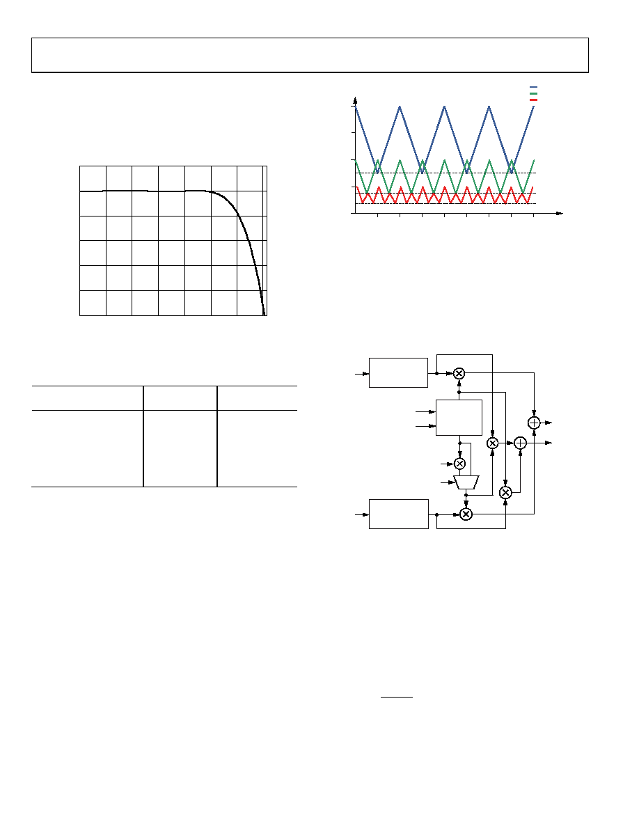
Figure 69 shows the pass-band filter response for HB3. In most
applications, the usable bandwidth of the filter is limited by the
image suppression provided by the stop-band rejection and not
by the pass-band flatness. Table 24 shows the pass-band flatness
and stop-band rejection the HB3 filter supports at different
bandwidths.
0.02
0
–0.02
–0.04
–0.06
–0.08
–0.10
00.28
0.24
0.20
0.16
0.12
0.08
0.04
MA
G
N
IT
U
D
E
(d
B
)
(×
fIN3)
08
91
0-
0
68
Figure 69. Pass-Band Detail of HB3
Table 24. HB3 Pass-Band and Stop-Band Performance by
Bandwidth
Bandwidth (% of fIN3)
Pass-Band
Flatness (dB)
Stop-Band
Rejection (dB)
40
0.001
85
40.8
0.0014
80
42.4
0.002
70
45.6
0.0093
60
49.8
0.03
50
55.6
0.1
40
The maximum bandwidth can be achieved if the signal carrier
frequency is placed directly at the center of one of the filter
pass bands. In this case, the entire quadrature bandwidth of the
interpolation filter (0.8 × fDATA) is available. The available signal
bandwidth decreases as the carrier frequency of the signal moves
away from the center frequency of the filter. The worst-case
carrier frequency is one that falls directly between the center
frequency of two adjacent filters. Figure 70 shows how the
signal bandwidth changes as a function of placement in the
spectrum and interpolation rate.
0.4
0.3
0.2
0.1
CO
M
P
L
E
X
BW
(
×f
DA
C
)
DC
–1/2
1/2
–3/8
3/8
–1/4
1/4
–1/8
1/8
fC (×fDAC)
×2 MODE
×4 MODE
×8 MODE
CARRIER FREQUENCY
0.075
0.0375
0.15
0
08
91
0-
0
69
Figure 70. Complex Signal Bandwidth as a Function of Output Frequency
FINE MODULATION
The fine modulation makes use of a numerically controlled oscillator,
a phase shifter, and a complex modulator to provide a means for
modulating the signal by a programmable carrier signal. A block
diagram of the fine modulator is shown in Figure 71. The fine
modulator allows the signal to be placed anywhere in the output
spectrum with very fine frequency resolution.
INTERPOLATION
NCO
1
0
–1
COSINE
SINE
I DATA
Q DATA
FTW[31:0]
SPECTRAL
INVERSION
OUT_I
OUT_Q
+
–
NCO PHASE OFFSET
WORD [15:0]
08910
-07
0
Figure 71. Fine Modulator Block Diagram
The quadrature modulator is used to mix the carrier signal
generated by the NCO with the I and Q signal. The NCO produces
a quadrature carrier signal to translate the input signal to a new
center frequency. A complex carrier signal is a pair of sinusoidal
waveforms of the same frequency, offset 90° from each other. The
frequency of the complex carrier signal is set via the FTW[31:0]
value in Register 0x54 through Register 0x57.
The NCO operating frequency, fNCO, is at the DAC rate. The
frequency of the complex carrier signal can be set from dc up
to fDAC/2. The frequency tuning word (FTW) is calculated as
32
2
DAC
CENTER
f
FTW
The generated quadrature carrier signal is mixed with the I and Q
data. The quadrature products are then summed into the I and
Q data paths, as shown in Figure 71.
相关PDF资料 |
PDF描述 |
|---|---|
| MS27473T10B98PBLC | CONN HSG PLUG 6POS STRGHT PINS |
| LTC2758ACLX#PBF | IC DAC 18BIT SPI/SRL 48-LQFP |
| MS27468T15B19PLC | CONN HSG RCPT 19POS JAMNUT PINS |
| V24B5M200BF2 | CONVERTER MOD DC/DC 5V 200W |
| MS27656T23B35B | CONN HSG RCPT 100POS WALL MT SCK |
相关代理商/技术参数 |
参数描述 |
|---|---|
| AD9148BBPZRL | 功能描述:IC DAC 16BIT SPI/SRL 196BGA RoHS:是 类别:集成电路 (IC) >> 数据采集 - 数模转换器 系列:TxDAC+® 产品培训模块:Lead (SnPb) Finish for COTS Obsolescence Mitigation Program 标准包装:1,000 系列:- 设置时间:1µs 位数:8 数据接口:串行 转换器数目:8 电压电源:双 ± 功率耗散(最大):941mW 工作温度:0°C ~ 70°C 安装类型:表面贴装 封装/外壳:24-SOIC(0.295",7.50mm 宽) 供应商设备封装:24-SOIC W 包装:带卷 (TR) 输出数目和类型:8 电压,单极 采样率(每秒):* |
| AD9148BPCZ | 制造商:AD 制造商全称:Analog Devices 功能描述:Quad 16-Bit,1 GSPS, TxDAC+ Digital-to-Analog Converter |
| AD9148BPCZRL | 制造商:AD 制造商全称:Analog Devices 功能描述:Quad 16-Bit,1 GSPS, TxDAC+ Digital-to-Analog Converter |
| AD9148-EBZ | 功能描述:BOARD EVALUATION FOR AD9148 RoHS:是 类别:编程器,开发系统 >> 评估板 - 数模转换器 (DAC) 系列:TxDAC+® 产品培训模块:Lead (SnPb) Finish for COTS Obsolescence Mitigation Program 标准包装:1 系列:- DAC 的数量:4 位数:12 采样率(每秒):- 数据接口:串行,SPI? 设置时间:3µs DAC 型:电流/电压 工作温度:-40°C ~ 85°C 已供物品:板 已用 IC / 零件:MAX5581 |
| AD9148-M5372-EBZ | 功能描述:BOARD EVAL FOR AD9149, ADL5372 RoHS:是 类别:编程器,开发系统 >> 评估板 - 数模转换器 (DAC) 系列:* 产品培训模块:Lead (SnPb) Finish for COTS Obsolescence Mitigation Program 标准包装:1 系列:- DAC 的数量:4 位数:12 采样率(每秒):- 数据接口:串行,SPI? 设置时间:3µs DAC 型:电流/电压 工作温度:-40°C ~ 85°C 已供物品:板 已用 IC / 零件:MAX5581 |
发布紧急采购,3分钟左右您将得到回复。