- 您现在的位置:买卖IC网 > PDF目录10097 > AD9226ARSZ (Analog Devices Inc)IC ADC 12BIT 65MSPS 28-SSOP PDF资料下载
参数资料
| 型号: | AD9226ARSZ |
| 厂商: | Analog Devices Inc |
| 文件页数: | 10/28页 |
| 文件大小: | 0K |
| 描述: | IC ADC 12BIT 65MSPS 28-SSOP |
| 产品培训模块: | ADC Applications ADC Architectures ADC DC/AC Performance |
| 标准包装: | 1 |
| 位数: | 12 |
| 采样率(每秒): | 65M |
| 数据接口: | 并联 |
| 转换器数目: | 3 |
| 功率耗散(最大): | 475mW |
| 电压电源: | 单电源 |
| 工作温度: | -40°C ~ 85°C |
| 安装类型: | 表面贴装 |
| 封装/外壳: | 28-SSOP(0.209",5.30mm 宽) |
| 供应商设备封装: | 28-SSOP |
| 包装: | 管件 |
| 输入数目和类型: | 2 个单端,单极;1 个差分,单极 |
第1页第2页第3页第4页第5页第6页第7页第8页第9页当前第10页第11页第12页第13页第14页第15页第16页第17页第18页第19页第20页第21页第22页第23页第24页第25页第26页第27页第28页
REV. B
AD9226
–18–
A2
LOGIC
A1
DISABLE
A1
1V
TO
A/D
AD9226
CAPT
CAPB
VREF
SENSE
REFCOM
2.5V
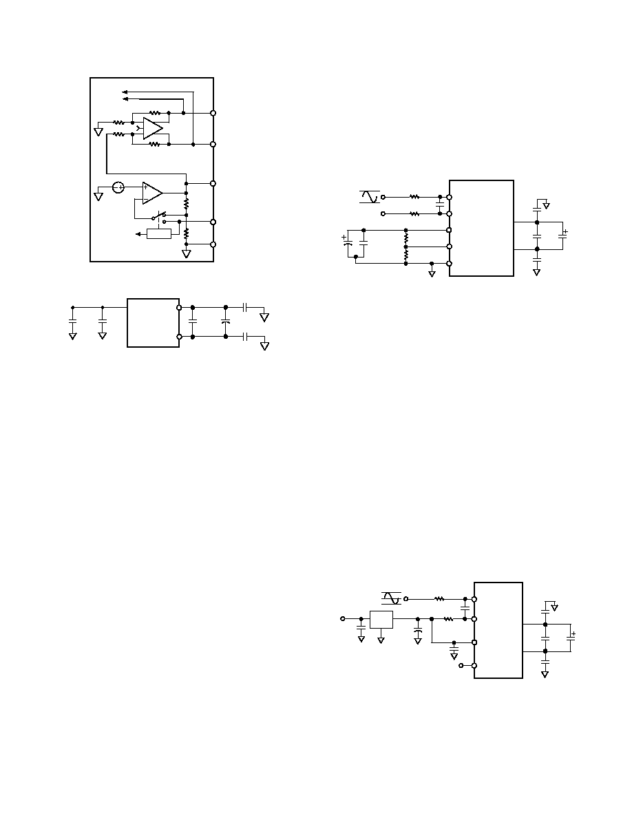
Figure 11a. Equivalent Reference Circuit
0.1 F
10 F
0.1 F
CAPT
CAPB
AD9226
VREF
0.1 F
10 F
Figure 11b. CAPT and CAPB DC-Coupling
The actual reference voltages used by the internal circuitry of the
AD9226 appear on the CAPT and CAPB pins. The voltages
on these pins are symmetrical about the analog supply. For
proper operation when using an internal or external reference, it
is necessary to add a capacitor network to decouple these pins.
Figure 11b shows the recommended decoupling network. The
turn-on time of the reference voltage appearing between CAPT
and CAPB is approximately 10 ms and should be evaluated in
any power-down mode of operation.
USING THE INTERNAL REFERENCE
The AD9226 can be easily configured for either a 1 V p-p input
span or 2 V p-p input span by setting the internal reference.
Other input spans can be realized with two external gain-
setting resistors as shown in Figure 12 of this data sheet, or
using an external reference.
Pin Programmable Reference
By shorting the VREF pin directly to the SENSE pin, the inter-
nal reference amplifier is placed in a unity-gain mode and the
resultant VREF output is 1 V. By shorting the SENSE pin
directly to the REFCOM pin, the internal reference amplifier is
configured for a gain of 2.0 and the resultant VREF output is
2.0 V. The VREF pin should be bypassed to the REFCOM pin
with a 10
F tantalum capacitor in parallel with a low-inductance
0.1
F ceramic capacitor as shown in Figure 11b.
Resistor Programmable Reference
Figure 12 shows an example of how to generate a reference
voltage other than 1.0 V or 2.0 V with the addition of two exter-
nal resistors. Use the equation,
VREF = 1 V
× (1 + R1/R2)
to determine appropriate values for R1 and R2. These resistors
should be in the 2 k
to 10 k range. For the example shown,
R1 equals 2.5 k
and R2 equals 5 k. From the equation above,
the resultant reference voltage on the VREF pin is 1.5 V. This
sets the input span to be 1.5 V p-p. The midscale voltage can
also be set to VREF by connecting VINB to VREF. Alterna-
tively, the midscale voltage can be set to 2.5 V by connecting
VINB to a low-impedance 2.5 V source as shown in Figure 12.
VINA
VREF
AD9226
VINB
1.75V
SENSE
REFCOM
0.1 F
10 F
0.1 F
15pF
3.25V
33
1.5V
0.1 F
CAPT
2.5V
10 F
R1
2.5k
R2
5k
CAPB
Figure 12. Resistor Programmable Reference (1.5 V p-p
Input Span, Differential Input VCM = 2.5 V)
USING AN EXTERNAL REFERENCE
The AD9226 contains an internal reference buffer, A2 (see
Figure 11b), that simplifies the drive requirements of an external
reference. The external reference must be able to drive about
5k
(±20%) load. Note that the bandwidth of the reference
buffer is deliberately left small to minimize the reference noise
contribution. As a result, it is not possible to rapidly change the
reference voltage in this mode.
Figure 13 shows an example of an external reference driving
both VINB and VREF. In this case, both the common-mode
voltage and input span are directly dependent on the value of
VREF. Both the input span and the center of the input span are
equal to the external VREF. Thus the valid input range extends
from (VREF + VREF/2) to (VREF – VREF/2). For example,
if the REF191, a 2.048 V external reference, is selected, the
input span extends to 2.048 V. In this case, 1 LSB of the AD9226
corresponds to 0.5 mV. It is essential that a minimum of a 10
F
capacitor, in parallel with a 0.1
F low-inductance ceramic
capacitor, decouple the reference output to ground.
To use an external reference, the SENSE pin must be connected
to AVDD. This connection will disable the internal reference.
VINA
VREF
AD9226
VINB
SENSE
0.1 F
10 F
0.1 F
15pF
VINA+VREF/2
33
0.1 F
CAPT
CAPB
VINB–VREF/2
10 F
VREF
0.1 F
5V
Figure 13. Using an External Reference
相关PDF资料 |
PDF描述 |
|---|---|
| LT1140ACSW | IC 5DRV/3RCV RS232 5V 24-SOIC |
| VE-263-MX-F2 | CONVERTER MOD DC/DC 24V 75W |
| VI-20Y-MY | CONVERTER MOD DC/DC 3.3V 33W |
| MS3106F28-19S | CONN PLUG 10POS STRAIGHT W/SCKT |
| IDT72225LB25TFI8 | IC FIFO 1024X18 SYNC 25NS 64TQFP |
相关代理商/技术参数 |
参数描述 |
|---|---|
| AD9226ARSZRL | 功能描述:IC ADC 12BIT 65MSPS 28SSOP RoHS:是 类别:集成电路 (IC) >> 数据采集 - 模数转换器 系列:- 标准包装:1 系列:- 位数:14 采样率(每秒):83k 数据接口:串行,并联 转换器数目:1 功率耗散(最大):95mW 电压电源:双 ± 工作温度:0°C ~ 70°C 安装类型:通孔 封装/外壳:28-DIP(0.600",15.24mm) 供应商设备封装:28-PDIP 包装:管件 输入数目和类型:1 个单端,双极 |
| AD9226AST | 功能描述:IC ADC 12BIT 65MSPS 48-LQFP RoHS:否 类别:集成电路 (IC) >> 数据采集 - 模数转换器 系列:- 产品培训模块:Lead (SnPb) Finish for COTS Obsolescence Mitigation Program 标准包装:2,500 系列:- 位数:12 采样率(每秒):3M 数据接口:- 转换器数目:- 功率耗散(最大):- 电压电源:- 工作温度:- 安装类型:表面贴装 封装/外壳:SOT-23-6 供应商设备封装:SOT-23-6 包装:带卷 (TR) 输入数目和类型:- |
| AD9226ASTRL | 功能描述:IC ADC 12BIT 65MSPS 48-LQFP RoHS:否 类别:集成电路 (IC) >> 数据采集 - 模数转换器 系列:- 产品培训模块:Lead (SnPb) Finish for COTS Obsolescence Mitigation Program 标准包装:2,500 系列:- 位数:12 采样率(每秒):3M 数据接口:- 转换器数目:- 功率耗散(最大):- 电压电源:- 工作温度:- 安装类型:表面贴装 封装/外壳:SOT-23-6 供应商设备封装:SOT-23-6 包装:带卷 (TR) 输入数目和类型:- |
| AD9226ASTZ | 功能描述:IC ADC 12BIT 65MSPS 48-LQFP RoHS:是 类别:集成电路 (IC) >> 数据采集 - 模数转换器 系列:- 标准包装:1 系列:microPOWER™ 位数:8 采样率(每秒):1M 数据接口:串行,SPI? 转换器数目:1 功率耗散(最大):- 电压电源:模拟和数字 工作温度:-40°C ~ 125°C 安装类型:表面贴装 封装/外壳:24-VFQFN 裸露焊盘 供应商设备封装:24-VQFN 裸露焊盘(4x4) 包装:Digi-Reel® 输入数目和类型:8 个单端,单极 产品目录页面:892 (CN2011-ZH PDF) 其它名称:296-25851-6 |
| AD9226ASTZRL | 功能描述:IC ADC 12BIT 65MSPS 48LQFP RoHS:是 类别:集成电路 (IC) >> 数据采集 - 模数转换器 系列:- 标准包装:1 系列:- 位数:14 采样率(每秒):83k 数据接口:串行,并联 转换器数目:1 功率耗散(最大):95mW 电压电源:双 ± 工作温度:0°C ~ 70°C 安装类型:通孔 封装/外壳:28-DIP(0.600",15.24mm) 供应商设备封装:28-PDIP 包装:管件 输入数目和类型:1 个单端,双极 |
发布紧急采购,3分钟左右您将得到回复。