- 您现在的位置:买卖IC网 > PDF目录10097 > AD9226ARSZ (Analog Devices Inc)IC ADC 12BIT 65MSPS 28-SSOP PDF资料下载
参数资料
| 型号: | AD9226ARSZ |
| 厂商: | Analog Devices Inc |
| 文件页数: | 11/28页 |
| 文件大小: | 0K |
| 描述: | IC ADC 12BIT 65MSPS 28-SSOP |
| 产品培训模块: | ADC Applications ADC Architectures ADC DC/AC Performance |
| 标准包装: | 1 |
| 位数: | 12 |
| 采样率(每秒): | 65M |
| 数据接口: | 并联 |
| 转换器数目: | 3 |
| 功率耗散(最大): | 475mW |
| 电压电源: | 单电源 |
| 工作温度: | -40°C ~ 85°C |
| 安装类型: | 表面贴装 |
| 封装/外壳: | 28-SSOP(0.209",5.30mm 宽) |
| 供应商设备封装: | 28-SSOP |
| 包装: | 管件 |
| 输入数目和类型: | 2 个单端,单极;1 个差分,单极 |
第1页第2页第3页第4页第5页第6页第7页第8页第9页第10页当前第11页第12页第13页第14页第15页第16页第17页第18页第19页第20页第21页第22页第23页第24页第25页第26页第27页第28页
REV. B
AD9226
–19–
MODE CONTROLS
Clock Stabilizer
The clock stabilizer is a circuit that desensitizes the ADC from
clock duty cycle variations. The AD9226 eases system clock
constraints by incorporating a circuit that restores the internal duty
cycle to 50%, independent of the input duty cycle. Low jitter on
the rising edge (sampling edge) of the clock is preserved while
the noncritical falling edge is generated on-chip.
It may be desirable to disable the clock stabilizer, and may be
necessary when the clock frequency speed is varied or completely
stopped. Once the clock frequency is changed, over 100 clock
cycles may be required for the clock stabilizer to settle to a dif-
ferent speed. When the stabilizer is disabled, the internal switching
will be directly affected by the clock state. If the external clock is
high, the SHA will be in hold. If the clock pulse is low, the SHA
will be in track. TPC 16 shows the benefits of using the clock
stabilizer. See Tables I and III.
Data Format Select (DFS)
The AD9226 may be set for binary or two’s complement data
output formats. See Tables I and II.
SSOP Package
The SSOP mode control (Pin 22) has two functions. It enables/
disables the clock stabilizer and determines the output data format.
The exact functions of the mode pin are outlined in Table I.
Table I. Mode Select (SSOP)
Mode
DFS
Clock Duty Cycle Shaping
DNC
Binary
Clock Stabilizer Disabled
AVDD
Binary
Clock Stabilizer Enabled
GND
Two’s Complement
Clock Stabilizer Enabled
10 k
Two’s Complement
Clock Stabilizer Disabled
Resistor
To GND
LQFP Package
Pin 35 of the LQFP package determines the output data format
(DFS). If it is connected to AVSS, the output word will be straight
binary. If it is connected to AVDD, the output data format will
be two’s complement. See Table II.
Pin 43 of the LQFP package controls the clock stabilizer function
of the AD9226. If the pin is connected to AVSS, both clock
edges will be used in the conversion architecture. When Pin 43
is connected to AVDD, the internal duty cycle will be determined
by the clock stabilizer function within the ADC. See Table III.
Table II. DFS Pin Controls
DFS Function
Pin 35 Connection
Straight Binary
AVSS
Two’s Complement
AVDD
Table III. Clock Stabilizer Pin
Clock Restore Function
Pin 43 Connection
Clock Stabilizer Enabled
AVDD
Clock Stabilizer Disabled
AVSS
DIGITAL INPUTS AND OUTPUTS
Digital Outputs
Table IV details the relationship among the ADC input, OTR, and
straight binary output.
Table IV. Output Data Format
Two’s
Binary
Complement
Input (V)
Condition (V)
Output Mode
Mode
OTR
VINA–VINB < – VREF
0000 0000 0000
1000 0000 0000
1
VINA–VINB = – VREF
0000 0000 0000
1000 0000 0000
0
VINA–VINB = 0
1000 0000 0000
0000 0000 0000
0
VINA–VINB = + VREF – 1 LSB 1111 1111 1111
0111 1111 1111
0
VINA–VINB
≥ + VREF
1111 1111 1111
0111 1111 1111
1
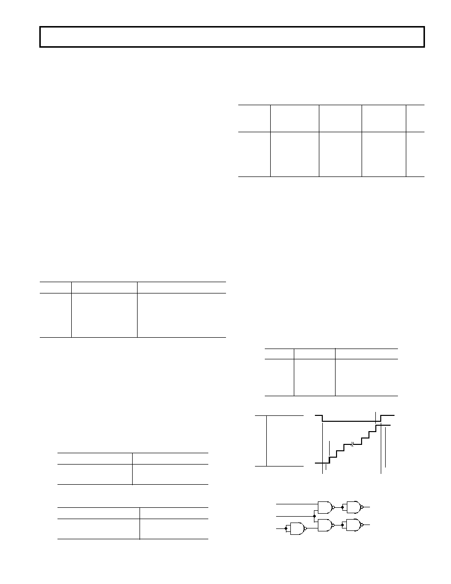
Out of Range (OTR)
An out-of-range condition exists when the analog input voltage
is beyond the input range of the converter. OTR is a digital
output that is updated along with the data output corresponding
to the particular sampled analog input voltage. Hence, OTR has
the same pipeline delay (latency) as the digital data. It is LOW
when the analog input voltage is within the analog input range.
It is HIGH when the analog input voltage exceeds the input
range as shown in Figure 14. OTR will remain HIGH until the
analog input returns within the input range and another conversion
is completed. By logical ANDing OTR with the MSB and its
complement, overrange high or underrange low conditions can be
detected. Table V is a truth table for the over/underrange
circuit in Figure 15, which uses NAND gates. Systems requiring
programmable gain conditioning of the AD9226 input signal
can immediately detect an out-of-range condition, thus elimi-
nating gain selection iterations. Also, OTR can be used for
digital offset and gain calibration.
Table V. Out-of-Range Truth Table
OTR
MSB
Analog Input Is
0
In Range
0
1
In Range
1
0
Underrange
1
Overrange
1111 1111 1111
1111 1111 1110
OTR
–FS
+FS
–FS +1/2 LSB
+FS – 1/2 LSB
–FS – 1/2 LSB
+FS – 1 1/2 LSB
0000 0000 0001
0000 0000 0000
1
0
1
OTR DATA OUTPUTS
Figure 14. OTR Relation to Input Voltage and Output Data
OVER = 1
UNDER = 1
MSB
OTR
MSB
Figure 15. Overrange or Underrange Logic
相关PDF资料 |
PDF描述 |
|---|---|
| LT1140ACSW | IC 5DRV/3RCV RS232 5V 24-SOIC |
| VE-263-MX-F2 | CONVERTER MOD DC/DC 24V 75W |
| VI-20Y-MY | CONVERTER MOD DC/DC 3.3V 33W |
| MS3106F28-19S | CONN PLUG 10POS STRAIGHT W/SCKT |
| IDT72225LB25TFI8 | IC FIFO 1024X18 SYNC 25NS 64TQFP |
相关代理商/技术参数 |
参数描述 |
|---|---|
| AD9226ARSZRL | 功能描述:IC ADC 12BIT 65MSPS 28SSOP RoHS:是 类别:集成电路 (IC) >> 数据采集 - 模数转换器 系列:- 标准包装:1 系列:- 位数:14 采样率(每秒):83k 数据接口:串行,并联 转换器数目:1 功率耗散(最大):95mW 电压电源:双 ± 工作温度:0°C ~ 70°C 安装类型:通孔 封装/外壳:28-DIP(0.600",15.24mm) 供应商设备封装:28-PDIP 包装:管件 输入数目和类型:1 个单端,双极 |
| AD9226AST | 功能描述:IC ADC 12BIT 65MSPS 48-LQFP RoHS:否 类别:集成电路 (IC) >> 数据采集 - 模数转换器 系列:- 产品培训模块:Lead (SnPb) Finish for COTS Obsolescence Mitigation Program 标准包装:2,500 系列:- 位数:12 采样率(每秒):3M 数据接口:- 转换器数目:- 功率耗散(最大):- 电压电源:- 工作温度:- 安装类型:表面贴装 封装/外壳:SOT-23-6 供应商设备封装:SOT-23-6 包装:带卷 (TR) 输入数目和类型:- |
| AD9226ASTRL | 功能描述:IC ADC 12BIT 65MSPS 48-LQFP RoHS:否 类别:集成电路 (IC) >> 数据采集 - 模数转换器 系列:- 产品培训模块:Lead (SnPb) Finish for COTS Obsolescence Mitigation Program 标准包装:2,500 系列:- 位数:12 采样率(每秒):3M 数据接口:- 转换器数目:- 功率耗散(最大):- 电压电源:- 工作温度:- 安装类型:表面贴装 封装/外壳:SOT-23-6 供应商设备封装:SOT-23-6 包装:带卷 (TR) 输入数目和类型:- |
| AD9226ASTZ | 功能描述:IC ADC 12BIT 65MSPS 48-LQFP RoHS:是 类别:集成电路 (IC) >> 数据采集 - 模数转换器 系列:- 标准包装:1 系列:microPOWER™ 位数:8 采样率(每秒):1M 数据接口:串行,SPI? 转换器数目:1 功率耗散(最大):- 电压电源:模拟和数字 工作温度:-40°C ~ 125°C 安装类型:表面贴装 封装/外壳:24-VFQFN 裸露焊盘 供应商设备封装:24-VQFN 裸露焊盘(4x4) 包装:Digi-Reel® 输入数目和类型:8 个单端,单极 产品目录页面:892 (CN2011-ZH PDF) 其它名称:296-25851-6 |
| AD9226ASTZRL | 功能描述:IC ADC 12BIT 65MSPS 48LQFP RoHS:是 类别:集成电路 (IC) >> 数据采集 - 模数转换器 系列:- 标准包装:1 系列:- 位数:14 采样率(每秒):83k 数据接口:串行,并联 转换器数目:1 功率耗散(最大):95mW 电压电源:双 ± 工作温度:0°C ~ 70°C 安装类型:通孔 封装/外壳:28-DIP(0.600",15.24mm) 供应商设备封装:28-PDIP 包装:管件 输入数目和类型:1 个单端,双极 |
发布紧急采购,3分钟左右您将得到回复。