- 您现在的位置:买卖IC网 > PDF目录10097 > AD9226ARSZ (Analog Devices Inc)IC ADC 12BIT 65MSPS 28-SSOP PDF资料下载
参数资料
| 型号: | AD9226ARSZ |
| 厂商: | Analog Devices Inc |
| 文件页数: | 8/28页 |
| 文件大小: | 0K |
| 描述: | IC ADC 12BIT 65MSPS 28-SSOP |
| 产品培训模块: | ADC Applications ADC Architectures ADC DC/AC Performance |
| 标准包装: | 1 |
| 位数: | 12 |
| 采样率(每秒): | 65M |
| 数据接口: | 并联 |
| 转换器数目: | 3 |
| 功率耗散(最大): | 475mW |
| 电压电源: | 单电源 |
| 工作温度: | -40°C ~ 85°C |
| 安装类型: | 表面贴装 |
| 封装/外壳: | 28-SSOP(0.209",5.30mm 宽) |
| 供应商设备封装: | 28-SSOP |
| 包装: | 管件 |
| 输入数目和类型: | 2 个单端,单极;1 个差分,单极 |
第1页第2页第3页第4页第5页第6页第7页当前第8页第9页第10页第11页第12页第13页第14页第15页第16页第17页第18页第19页第20页第21页第22页第23页第24页第25页第26页第27页第28页
REV. B
AD9226
–16–
1V p-p
VINA
CAPB
AD9226
0.1 F
1k
49.9
499
0.1 F
10 F
0.1 F
CAPT
0.1 F
450
VINB
AD8138
10 F
AVDD
0.1 F
10 F
5V
0.1 F
1k
0V
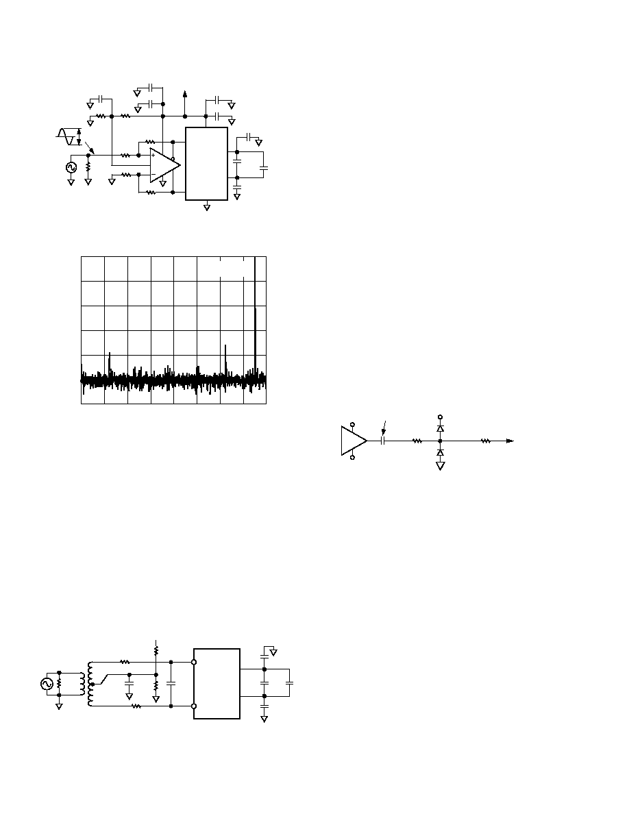
Figure 6a. Direct-Coupled Drive Circuit with AD8138
Differential Op Amp
0
–20
–40
–60
–80
–100
–120
04
8
12
16
20
24
28
32
MHz
SNR = 66.9dBc
SFDR = 70.0dBc
dBc
Figure 6b. FS = 65 MSPS, fIN = 30 MHz, Input Span = 1 V p-p
The same midsupply potential may be obtained from the
CMLEVEL pin of the AD9226 in the LQFP package.
Referring to Figure 7, a series resistor, RS, is inserted between the
AD9226 and the secondary of the transformer. The value of
33 ohm was selected to specifically optimize both the THD and
SNR performance of the ADC. RS and the internal capacitance
help provide a low-pass filter to block high-frequency noise.
Transformers with other turns ratios may also be selected to
optimize the performance of a given application. For example, a
given input signal source or amplifier may realize an improve-
ment in distortion performance at reduced output power levels
and signal swings. By selecting a transformer with a higher
impedance ratio (e.g., Minicircuits T16-6T with a 1:16 imped-
ance ratio), the signal level is effectively “stepped up” thus
further reducing the driving requirements of signal source.
VINA
VINB
AD9226
49.9
RS
33
MINICIRCUITS
T1-1T
0.1 F
RS
33
0.1 F
10 F
0.1 F
CAPB
CAPT
15pF
1k
AVDD
Figure 7. Transformer-Coupled Input
SINGLE-ENDED DRIVER CIRCUITS
The AD9226 can be configured for single-ended operation using
dc- or ac-coupling. In either case, the input of the ADC must be
driven from an operational amplifier that will not degrade the
ADC’s performance. Because the ADC operates from a single
supply, it will be necessary to level-shift ground-based bipolar
signals to comply with its input requirements. Both dc- and
ac-coupling provide this necessary function, but each method
results in different interface issues which may influence the
system design and performance.
Single-ended operation requires that VINA be ac- or dc-coupled
to the input signal source, while VINB of the AD9226 be biased
to the appropriate voltage corresponding to the middle of the input
span. The single-ended specifications for the AD9226 are char-
acterized using Figure 9a circuitry with input spans of 1 V and
2 V. The common-mode level is 2.5 V.
If the analog inputs exceed the supply limits, internal parasitic
diodes will turn on. This will result in transient currents within
the device. Figure 8 shows a simple means of clamping an input.
It uses a series resistor and two diodes. An optional capacitor is
shown for ac-coupled applications. A larger series resistor can
be used to limit the fault current through D1 and D2. This
can cause a degradation in overall performance. A similar
clamping circuit can also be used for each input if a differen-
tial input signal is being applied. A better method to ensure
the input is not overdriven is to use amplifiers powered by a single
5 V supply such as the AD8138.
AVDD
AD9226
RS1
30
VCC
VEE
OPTIONAL
AC-COUPLING
CAPACITOR
D2
D1
RS2
20
Figure 8. Simple Clamping Circuit
AC-COUPLING AND INTERFACE ISSUES
For applications where ac-coupling is appropriate, the op amp
output can be easily level-shifted by means of a coupling
capacitor. This has the advantage of allowing the op amp’s com-
mon-mode level to be symmetrically biased to its midsupply
level (i.e., (AVDD/2). Op amps that operate symmetrically with
respect to their power supplies typically provide the best ac
performance as well as greatest input/output span. Various high-
speed performance amplifiers that are restricted to +5 V/–5 V
operation and/or specified for 5 V single-supply operation can be
easily configured for the 2 V or 1 V input span of the AD9226.
Simple AC Interface
Figure 9a shows a typical example of an ac-coupled, single-
ended configuration of the SSOP package. The bias voltage
shifts the bipolar, ground-referenced input signal to approxi-
mately AVDD/2. The capacitors, C1 and C2, are 0.1
F ceramic
and 10
F tantalum capacitors in parallel to achieve a low
cutoff frequency while maintaining a low impedance over a
wide frequency range. The combination of the capacitor and the
resistor form a high-pass network with a high-pass –3 dB fre-
quency determined by the equation,
f–3 dB = 1/(2
× π × R × (C1 + C2))
相关PDF资料 |
PDF描述 |
|---|---|
| LT1140ACSW | IC 5DRV/3RCV RS232 5V 24-SOIC |
| VE-263-MX-F2 | CONVERTER MOD DC/DC 24V 75W |
| VI-20Y-MY | CONVERTER MOD DC/DC 3.3V 33W |
| MS3106F28-19S | CONN PLUG 10POS STRAIGHT W/SCKT |
| IDT72225LB25TFI8 | IC FIFO 1024X18 SYNC 25NS 64TQFP |
相关代理商/技术参数 |
参数描述 |
|---|---|
| AD9226ARSZRL | 功能描述:IC ADC 12BIT 65MSPS 28SSOP RoHS:是 类别:集成电路 (IC) >> 数据采集 - 模数转换器 系列:- 标准包装:1 系列:- 位数:14 采样率(每秒):83k 数据接口:串行,并联 转换器数目:1 功率耗散(最大):95mW 电压电源:双 ± 工作温度:0°C ~ 70°C 安装类型:通孔 封装/外壳:28-DIP(0.600",15.24mm) 供应商设备封装:28-PDIP 包装:管件 输入数目和类型:1 个单端,双极 |
| AD9226AST | 功能描述:IC ADC 12BIT 65MSPS 48-LQFP RoHS:否 类别:集成电路 (IC) >> 数据采集 - 模数转换器 系列:- 产品培训模块:Lead (SnPb) Finish for COTS Obsolescence Mitigation Program 标准包装:2,500 系列:- 位数:12 采样率(每秒):3M 数据接口:- 转换器数目:- 功率耗散(最大):- 电压电源:- 工作温度:- 安装类型:表面贴装 封装/外壳:SOT-23-6 供应商设备封装:SOT-23-6 包装:带卷 (TR) 输入数目和类型:- |
| AD9226ASTRL | 功能描述:IC ADC 12BIT 65MSPS 48-LQFP RoHS:否 类别:集成电路 (IC) >> 数据采集 - 模数转换器 系列:- 产品培训模块:Lead (SnPb) Finish for COTS Obsolescence Mitigation Program 标准包装:2,500 系列:- 位数:12 采样率(每秒):3M 数据接口:- 转换器数目:- 功率耗散(最大):- 电压电源:- 工作温度:- 安装类型:表面贴装 封装/外壳:SOT-23-6 供应商设备封装:SOT-23-6 包装:带卷 (TR) 输入数目和类型:- |
| AD9226ASTZ | 功能描述:IC ADC 12BIT 65MSPS 48-LQFP RoHS:是 类别:集成电路 (IC) >> 数据采集 - 模数转换器 系列:- 标准包装:1 系列:microPOWER™ 位数:8 采样率(每秒):1M 数据接口:串行,SPI? 转换器数目:1 功率耗散(最大):- 电压电源:模拟和数字 工作温度:-40°C ~ 125°C 安装类型:表面贴装 封装/外壳:24-VFQFN 裸露焊盘 供应商设备封装:24-VQFN 裸露焊盘(4x4) 包装:Digi-Reel® 输入数目和类型:8 个单端,单极 产品目录页面:892 (CN2011-ZH PDF) 其它名称:296-25851-6 |
| AD9226ASTZRL | 功能描述:IC ADC 12BIT 65MSPS 48LQFP RoHS:是 类别:集成电路 (IC) >> 数据采集 - 模数转换器 系列:- 标准包装:1 系列:- 位数:14 采样率(每秒):83k 数据接口:串行,并联 转换器数目:1 功率耗散(最大):95mW 电压电源:双 ± 工作温度:0°C ~ 70°C 安装类型:通孔 封装/外壳:28-DIP(0.600",15.24mm) 供应商设备封装:28-PDIP 包装:管件 输入数目和类型:1 个单端,双极 |
发布紧急采购,3分钟左右您将得到回复。