- 您现在的位置:买卖IC网 > PDF目录10097 > AD9226ARSZ (Analog Devices Inc)IC ADC 12BIT 65MSPS 28-SSOP PDF资料下载
参数资料
| 型号: | AD9226ARSZ |
| 厂商: | Analog Devices Inc |
| 文件页数: | 14/28页 |
| 文件大小: | 0K |
| 描述: | IC ADC 12BIT 65MSPS 28-SSOP |
| 产品培训模块: | ADC Applications ADC Architectures ADC DC/AC Performance |
| 标准包装: | 1 |
| 位数: | 12 |
| 采样率(每秒): | 65M |
| 数据接口: | 并联 |
| 转换器数目: | 3 |
| 功率耗散(最大): | 475mW |
| 电压电源: | 单电源 |
| 工作温度: | -40°C ~ 85°C |
| 安装类型: | 表面贴装 |
| 封装/外壳: | 28-SSOP(0.209",5.30mm 宽) |
| 供应商设备封装: | 28-SSOP |
| 包装: | 管件 |
| 输入数目和类型: | 2 个单端,单极;1 个差分,单极 |
第1页第2页第3页第4页第5页第6页第7页第8页第9页第10页第11页第12页第13页当前第14页第15页第16页第17页第18页第19页第20页第21页第22页第23页第24页第25页第26页第27页第28页
REV. B
AD9226
–21–
VR
VR is an internal bias point on the LQFP package. It must be
decoupled to ground with a 0.1
F capacitor.
The digital activity on the AD9226 chip falls into two general
categories: correction logic and output drivers. The internal
correction logic draws relatively small surges of current, mainly
during the clock transitions. The output drivers draw large
current impulses while the output bits are changing. The size
and duration of these currents are a function of the load on the
output bits: large capacitive loads are to be avoided.
For the digital decoupling shown in Figure 19, 0.1
F ceramic
chip and 10
F tantalum capacitors are appropriate. Reason-
able capacitive loads on the data pins are less than 20 pF per
bit. Applications involving greater digital loads should consider
increasing the digital decoupling proportionally and/or using
external buffers/latches.
A complete decoupling scheme will also include large tantalum
or electrolytic capacitors on the power supply connector to
reduce low-frequency ripple to negligible levels.
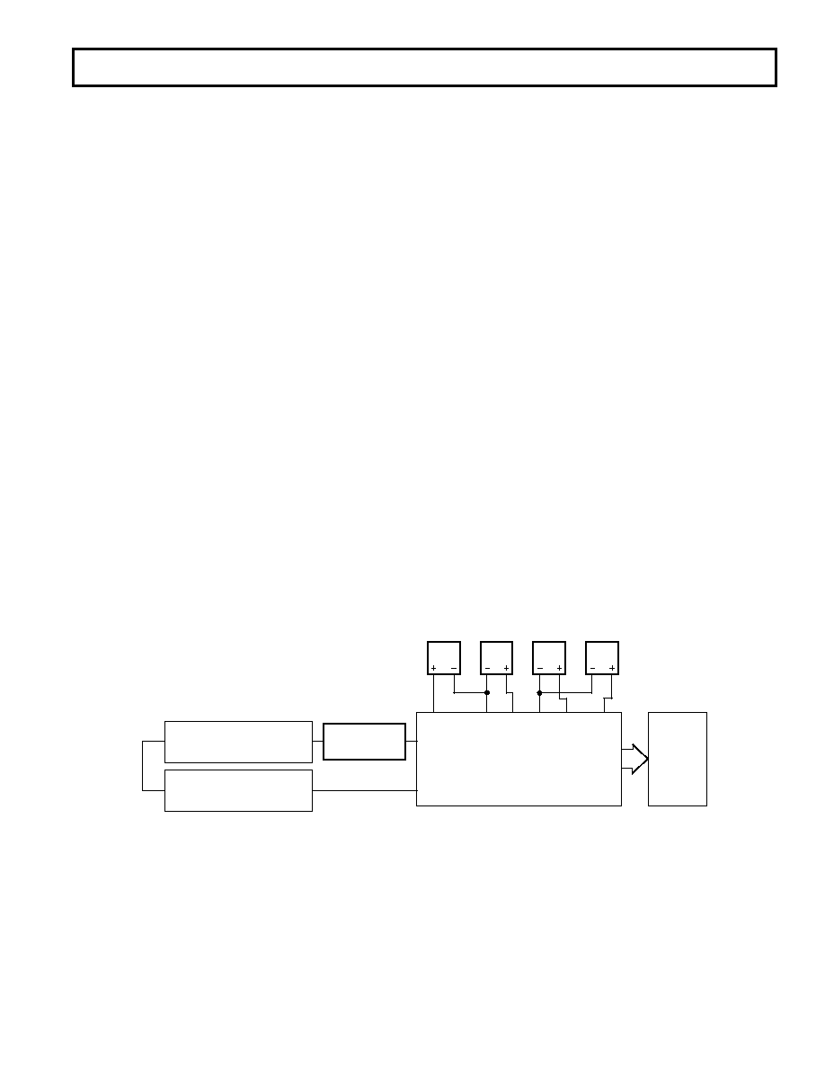
EVALUATION BOARD AND TYPICAL BENCH
CHARACTERIZATION TEST SETUP
The AD9226 evaluation board is configured to operate upon
applying both power and the analog and clock input signals. It
provides three possible analog input interfaces to characterize
the AD9226’s ac and dc performance. For ac characterization, it
provides a transformer coupled input with the common-mode
input voltage (CMV) set to AVDD/2. Note, the evaluation
board is shipped with a transformer coupled interface and a 2 V
input span. For differential dc coupled applications, the evalua-
tion board has provisions to be driven by the AD8138 amplifier.
If a single-ended input is desired, it may be driven through the
S3 connector. The various input signal options are accessible by
the jumper connections. Refer to the Evaluation Board schematic.
The clock input signal to the AD9226 evaluation board can be
applied to one of two inputs, CLOCK and AUXCLK. The
CLOCK input should be selected if the frequency of the input
clock signal is at the target sample rate of the AD9226. The
input clock signal is ac-coupled and level-shifted to the switch-
ing threshold of a 74VHC02 clock driver. The AUXCLK input
should be selected in applications requiring the lowest jitter and
SNR performance (i.e., IF Undersampling characterization). It
allows the user to apply a clock input signal that is 4
× the target
sample rate of the AD9226. A low-jitter, differential divide-by-4
counter, the MC100EL33D, provides a 1
× clock output that is
subsequently returned back to the CLOCK input via JP7. For
example, a 260 MHz signal (sinusoid) will be divided down to
a 65 MHz signal for clocking the ADC. Note, R1 must be
removed with the AUXCLK interface. Lower jitter is often
achieved with this interface since many RF signal generators
display improved phase noise at higher output frequencies and
the slew rate of the sinusoidal output signal is 4
× that of a 1×
signal of equal amplitude.
Figure 20 shows the bench characterization setup used to evalu-
ate the AD9226’s ac performance for many of the data sheet
characterization curves. Signal and Clock RF generators A and
B are high-frequency, “very” low-phase noise frequency sources.
These generators should be phase locked by sharing the same
10 MHz REF signal (located on the instruments back panel) to
allow for nonwindowed, coherent FFTs. Also, the AUXCLK
option on the AD9226 evaluation board should be used to
achieve the best SNR performance. Since the distortion and
broadband noise of an RF generator can often be a limiting
factor in measuring the true performance of an ADC, a high Q
passive bandpass filter should be inserted between the generator
and AD9226 evaluation board.
5V
3V
AVDD
GND
DUT
DVDD
DUT
AVDD
DSP
EQUIPMENT
S4
INPUT
xFMR
S1
INPUT
CLOCK
AD9226
EVALUATION BOARD
1MHz
BANDPASS FILTER
SIGNAL SYNTHESIZER
65(OR 260MHz), 4V p-p
HP8644
OUTPUT
WORD
(P1)
S4
AUX CLOCK
( 4)
REFIN
CLK SYNTHESIZER
65(OR 260MHz), 4V p-p
HP8644
10MHz
REFOUT
Figure 20. Evaluation Board Connections
相关PDF资料 |
PDF描述 |
|---|---|
| LT1140ACSW | IC 5DRV/3RCV RS232 5V 24-SOIC |
| VE-263-MX-F2 | CONVERTER MOD DC/DC 24V 75W |
| VI-20Y-MY | CONVERTER MOD DC/DC 3.3V 33W |
| MS3106F28-19S | CONN PLUG 10POS STRAIGHT W/SCKT |
| IDT72225LB25TFI8 | IC FIFO 1024X18 SYNC 25NS 64TQFP |
相关代理商/技术参数 |
参数描述 |
|---|---|
| AD9226ARSZRL | 功能描述:IC ADC 12BIT 65MSPS 28SSOP RoHS:是 类别:集成电路 (IC) >> 数据采集 - 模数转换器 系列:- 标准包装:1 系列:- 位数:14 采样率(每秒):83k 数据接口:串行,并联 转换器数目:1 功率耗散(最大):95mW 电压电源:双 ± 工作温度:0°C ~ 70°C 安装类型:通孔 封装/外壳:28-DIP(0.600",15.24mm) 供应商设备封装:28-PDIP 包装:管件 输入数目和类型:1 个单端,双极 |
| AD9226AST | 功能描述:IC ADC 12BIT 65MSPS 48-LQFP RoHS:否 类别:集成电路 (IC) >> 数据采集 - 模数转换器 系列:- 产品培训模块:Lead (SnPb) Finish for COTS Obsolescence Mitigation Program 标准包装:2,500 系列:- 位数:12 采样率(每秒):3M 数据接口:- 转换器数目:- 功率耗散(最大):- 电压电源:- 工作温度:- 安装类型:表面贴装 封装/外壳:SOT-23-6 供应商设备封装:SOT-23-6 包装:带卷 (TR) 输入数目和类型:- |
| AD9226ASTRL | 功能描述:IC ADC 12BIT 65MSPS 48-LQFP RoHS:否 类别:集成电路 (IC) >> 数据采集 - 模数转换器 系列:- 产品培训模块:Lead (SnPb) Finish for COTS Obsolescence Mitigation Program 标准包装:2,500 系列:- 位数:12 采样率(每秒):3M 数据接口:- 转换器数目:- 功率耗散(最大):- 电压电源:- 工作温度:- 安装类型:表面贴装 封装/外壳:SOT-23-6 供应商设备封装:SOT-23-6 包装:带卷 (TR) 输入数目和类型:- |
| AD9226ASTZ | 功能描述:IC ADC 12BIT 65MSPS 48-LQFP RoHS:是 类别:集成电路 (IC) >> 数据采集 - 模数转换器 系列:- 标准包装:1 系列:microPOWER™ 位数:8 采样率(每秒):1M 数据接口:串行,SPI? 转换器数目:1 功率耗散(最大):- 电压电源:模拟和数字 工作温度:-40°C ~ 125°C 安装类型:表面贴装 封装/外壳:24-VFQFN 裸露焊盘 供应商设备封装:24-VQFN 裸露焊盘(4x4) 包装:Digi-Reel® 输入数目和类型:8 个单端,单极 产品目录页面:892 (CN2011-ZH PDF) 其它名称:296-25851-6 |
| AD9226ASTZRL | 功能描述:IC ADC 12BIT 65MSPS 48LQFP RoHS:是 类别:集成电路 (IC) >> 数据采集 - 模数转换器 系列:- 标准包装:1 系列:- 位数:14 采样率(每秒):83k 数据接口:串行,并联 转换器数目:1 功率耗散(最大):95mW 电压电源:双 ± 工作温度:0°C ~ 70°C 安装类型:通孔 封装/外壳:28-DIP(0.600",15.24mm) 供应商设备封装:28-PDIP 包装:管件 输入数目和类型:1 个单端,双极 |
发布紧急采购,3分钟左右您将得到回复。