- 您现在的位置:买卖IC网 > PDF目录10663 > AD9241ASZ (Analog Devices Inc)IC ADC 14BIT 1.25MSPS 44-MQFP PDF资料下载
参数资料
| 型号: | AD9241ASZ |
| 厂商: | Analog Devices Inc |
| 文件页数: | 10/24页 |
| 文件大小: | 0K |
| 描述: | IC ADC 14BIT 1.25MSPS 44-MQFP |
| 标准包装: | 1 |
| 位数: | 14 |
| 采样率(每秒): | 1.25M |
| 数据接口: | 并联 |
| 转换器数目: | 7 |
| 功率耗散(最大): | 85mW |
| 电压电源: | 模拟和数字 |
| 工作温度: | -40°C ~ 85°C |
| 安装类型: | 表面贴装 |
| 封装/外壳: | 44-QFP |
| 供应商设备封装: | 44-MQFP(10x10) |
| 包装: | 托盘 |
| 输入数目和类型: | 2 个单端,单极;1 个差分,单极 |
| 产品目录页面: | 780 (CN2011-ZH PDF) |
AD9241
REV. 0
–18–
It is HIGH when the analog input voltage exceeds the input
range as shown in Figure 42. OTR will remain HIGH until the
analog input returns within the input range and another conver-
sion is completed. By logical ANDing OTR with the MSB and
its complement, overrange high or underrange low conditions
can be detected. Table V is a truth table for the over/underrange
circuit in Figure 43, which uses NAND gates. Systems requiring
programmable gain conditioning of the AD9241 input signal
can immediately detect an out-of-range condition, thus elimi-
nating gain selection iterations. Also, OTR can be used for
digital offset and gain calibration.
Table V. Out-of-Range Truth Table
OTR
MSB
Analog Input Is
0
In Range
0
1
In Range
1
0
Underrange
1
Overrange
OVER = “1”
UNDER = “1”
MSB
OTR
MSB
Figure 43. Overrange or Underrange Logic
Digital Output Driver Considerations (DRVDD)
The AD9241 output drivers can be configured to interface with
+5 V or 3.3 V logic families by setting DRVDD to +5 V or 3.3 V
respectively. The AD9241 output drivers are sized to provide
sufficient output current to drive a wide variety of logic families.
However, large drive currents tend to cause glitches on the
supplies and may affect SINAD performance. Applications
requiring the AD9241 to drive large capacitive loads or large
fanout may require additional decoupling capacitors on DRVDD.
In extreme cases, external buffers or latches may be required.
Clock Input and Considerations
The AD9241 internal timing uses the two edges of the clock
input to generate a variety of internal timing signals. The clock
input must meet or exceed the minimum specified pulse width
high and low (tCH and tCL) specifications for the given A/D, as
defined in the Switching Specifications section at the beginning
of the data sheet, to meet the rated performance specifications.
For example, the clock input to the AD9241 operating at 1.25
MSPS may have a duty cycle between 45% to 55% to meet this
timing requirement since the minimum specified tCH and tCL is
360 ns. For clock rates below 1.25 MSPS, the duty cycle may
deviate from this range to the extent that both tCH and tCL are
satisfied.
All high speed, high resolution A/Ds are sensitive to the quality
of the clock input. The degradation in SNR at a given full-scale
input frequency (fIN) due only to aperture jitter (tA) can be
calculated with the following equation:
SNR = 20 log10 [1/(2 π fIN tA)]
In the equation, the rms aperture jitter, tA, represents the root-
sum square of all the jitter sources including the clock input,
analog input signal and A/D aperture jitter specification. For
example, if a 1.0 MHz full-scale sine wave is sampled by an A/D
with a total rms jitter of 15 ps, the SNR performance of the A/D
will be limited to 80.5 dB. Undersampling applications are
particularly sensitive to jitter.
The clock input should be treated as an analog signal in cases
where aperture jitter may affect the dynamic range of the
AD9241. As such, supplies for clock drivers should be separated
from the A/D output driver supplies to avoid modulating the
clock signal with digital noise. Low jitter crystal controlled oscil-
lators make the best clock sources. If the clock is generated from
another type of source (by gating, dividing or other method), it
should be retimed by the original clock at the last step.
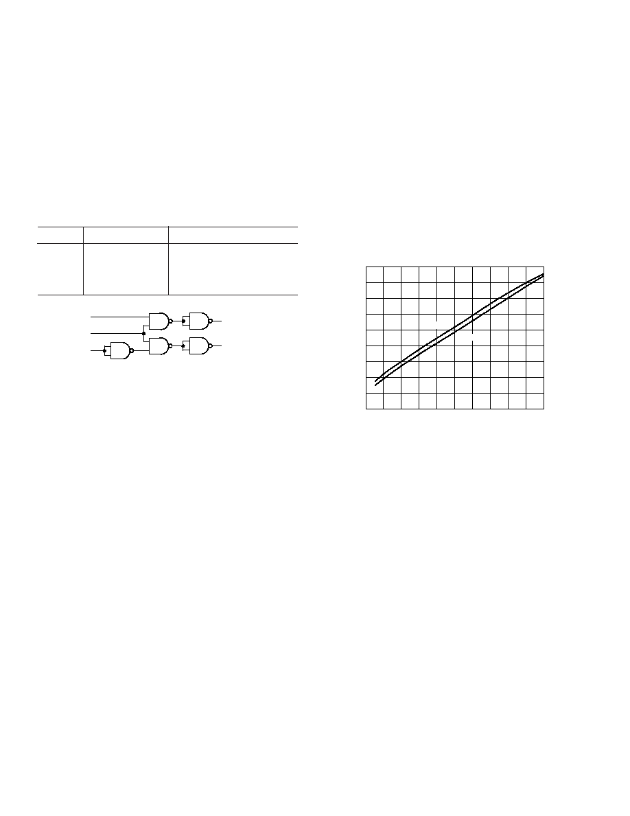
Most of the power dissipated by the AD9241 is from the analog
power supply. However, lower clock speeds will slightly reduce
digital current. Figure 44 shows the relationship between power
and clock rate.
CLOCK RATE – MHz
150
140
110
6
POWER
–
mW
5
130
120
5V p-p
2V p-p
100
90
80
4
3
2
1
0
70
60
789
10
Figure 44. AD9241 Power Consumption vs. Clock
Frequency
GROUNDING AND DECOUPLING
Analog and Digital Grounding
Proper grounding is essential in any high speed, high resolution
system. Multilayer printed circuit boards (PCBs) are recom-
mended to provide optimal grounding and power schemes. The
use of ground and power planes offers distinct advantages:
1. The minimization of the loop area encompassed by a signal
and its return path.
2. The minimization of the impedance associated with ground
and power paths.
3. The inherent distributed capacitor formed by the power
plane, PCB insulation and ground plane.
These characteristics result in both a reduction of electro-
magnetic interference (EMI) and an overall improvement in
performance.
It is important to design a layout that prevents noise from coupling
onto the input signal. Digital signals should not be run in paral-
lel with input signal traces, and should be routed away from the
input circuitry. While the AD9241 features separate analog and
digital ground pins, it should be treated as an analog compo-
nent. The AVSS, DVSS and DRVSS pins must be joined to-
gether directly under the AD9241. A solid ground plane under
the A/D is acceptable if the power and ground return currents
are carefully managed. Alternatively, the ground plane under
相关PDF资料 |
PDF描述 |
|---|---|
| MAX9140EUK-T | IC COMPARATOR SGL R-R LP SOT23-5 |
| MAX919EUK/V+T | IC COMPARATOR NANO 1.8V SOT23-5 |
| AD9224ARSZ | IC ADC 12BIT 40MSPS 28-SSOP |
| AD9238BSTZ-40 | IC ADC 12BIT DUAL 40MSPS 64-LQFP |
| VI-J13-MW-F2 | CONVERTER MOD DC/DC 24V 100W |
相关代理商/技术参数 |
参数描述 |
|---|---|
| AD9241ASZRL | 功能描述:IC ADC 14BIT SGL 1.25MSPS 44MQFP RoHS:是 类别:集成电路 (IC) >> 数据采集 - 模数转换器 系列:- 标准包装:1,000 系列:- 位数:12 采样率(每秒):300k 数据接口:并联 转换器数目:1 功率耗散(最大):75mW 电压电源:单电源 工作温度:0°C ~ 70°C 安装类型:表面贴装 封装/外壳:24-SOIC(0.295",7.50mm 宽) 供应商设备封装:24-SOIC 包装:带卷 (TR) 输入数目和类型:1 个单端,单极;1 个单端,双极 |
| AD9241EB | 制造商:AD 制造商全称:Analog Devices 功能描述:Complete 14-Bit, 1.25 MSPS Monolithic A/D Converter |
| AD9241-EB | 制造商:Analog Devices 功能描述:Evaluation Board For AD9241 制造商:Analog Devices 功能描述:EVAL BD FOR AD9241 - Bulk |
| AD9243 | 制造商:AD 制造商全称:Analog Devices 功能描述:Complete 14-Bit, 3.0 MSPS Monolithic A/D Converter |
发布紧急采购,3分钟左右您将得到回复。