- 您现在的位置:买卖IC网 > PDF目录10663 > AD9241ASZ (Analog Devices Inc)IC ADC 14BIT 1.25MSPS 44-MQFP PDF资料下载
参数资料
| 型号: | AD9241ASZ |
| 厂商: | Analog Devices Inc |
| 文件页数: | 11/24页 |
| 文件大小: | 0K |
| 描述: | IC ADC 14BIT 1.25MSPS 44-MQFP |
| 标准包装: | 1 |
| 位数: | 14 |
| 采样率(每秒): | 1.25M |
| 数据接口: | 并联 |
| 转换器数目: | 7 |
| 功率耗散(最大): | 85mW |
| 电压电源: | 模拟和数字 |
| 工作温度: | -40°C ~ 85°C |
| 安装类型: | 表面贴装 |
| 封装/外壳: | 44-QFP |
| 供应商设备封装: | 44-MQFP(10x10) |
| 包装: | 托盘 |
| 输入数目和类型: | 2 个单端,单极;1 个差分,单极 |
| 产品目录页面: | 780 (CN2011-ZH PDF) |
AD9241
REV. 0
–19–
the A/D may contain serrations to steer currents in predictable
directions where cross-coupling between analog and digital
would otherwise be unavoidable. The AD9241/EB ground lay-
out shown in Figure 52 depicts the serrated type of arrange-
ment. The analog and digital grounds are connected by a jumper
below the A/D.
Analog and Digital Supply Decoupling
The AD9241 features separate analog and digital supply and
ground pins, helping to minimize digital corruption of sensitive
analog signals.
FREQUENCY – kHz
120
PSRR
–
dBFS
100
1000
80
60
40
100
10
1
DVDD
AVDD
Figure 45. PSRR vs. Frequency
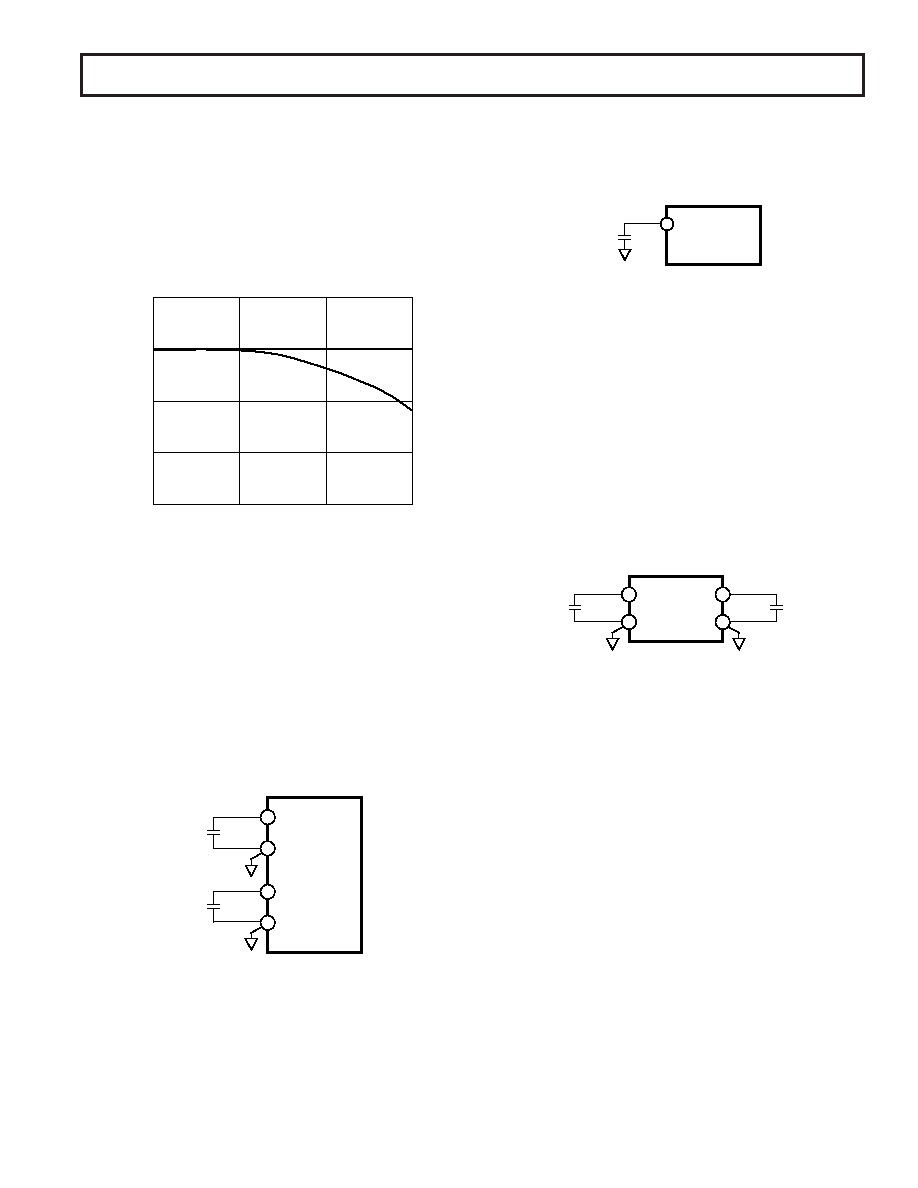
Figure 45 shows the power supply rejection ratio vs. frequency
for a 200 mV p-p ripple applied to both AVDD and DVDD.
In general, AVDD, the analog supply, should be decoupled to
AVSS, the analog common, as close to the chip as physically
possible. Figure 46 shows the recommended decoupling for the
analog supplies; 0.1
F ceramic chip capacitors should provide
adequately low impedance over a wide frequency range. Note
that the AVDD and AVSS pins are co-located on the AD9241
to simplify the layout of the decoupling capacitors and provide
the shortest possible PCB trace lengths. The AD9241/EB power
plane layout shown in Figure 53 depicts a typical arrangement
using a multilayer PCB.
0.1F
AVDD
AVSS
AD9241
0.1F
AVDD
AVSS
Figure 46. Analog Supply Decoupling
The CML is an internal analog bias point used internally by the
AD9241. This pin must be decoupled with at least a 0.1
F
capacitor as shown in Figure 47. The dc level of CML is ap-
proximately AVDD/2. This voltage should be buffered if it is to
be used for any external biasing.
0.1F
CML
AD9241
Figure 47. CML Decoupling
The digital activity on the AD9241 chip falls into two general
categories: correction logic and output drivers. The internal
correction logic draws relatively small surges of current, prima-
rily during the clock transitions. The output drivers draw large
current impulses while the output bits are changing. The size
and duration of these currents are a function of the load on the
output bits: large capacitive loads are to be avoided. Note that
the internal correction logic of the AD9241 is referenced DVDD
while the output drivers are referenced to DRVDD.
The decoupling shown in Figure 48 (a 0.1
F ceramic chip
capacitor) is appropriate for a reasonable capacitive load on the
digital outputs (typically 20 pF on each pin). Applications in-
volving greater digital loads should consider increasing the digi-
tal decoupling proportionally and/or using external buffers/
latches.
0.1F
DVDD
DVSS
AD9241
DRVDD
DRVSS
0.1F
Figure 48. Digital Supply Decoupling
A complete decoupling scheme will also include large tantalum
or electrolytic capacitors on the PCB to reduce low-frequency
ripple to negligible levels. Refer to the AD9241/EB schematic
and layouts in Figures 49–53 for more information regarding the
placement of decoupling capacitors.
相关PDF资料 |
PDF描述 |
|---|---|
| MAX9140EUK-T | IC COMPARATOR SGL R-R LP SOT23-5 |
| MAX919EUK/V+T | IC COMPARATOR NANO 1.8V SOT23-5 |
| AD9224ARSZ | IC ADC 12BIT 40MSPS 28-SSOP |
| AD9238BSTZ-40 | IC ADC 12BIT DUAL 40MSPS 64-LQFP |
| VI-J13-MW-F2 | CONVERTER MOD DC/DC 24V 100W |
相关代理商/技术参数 |
参数描述 |
|---|---|
| AD9241ASZRL | 功能描述:IC ADC 14BIT SGL 1.25MSPS 44MQFP RoHS:是 类别:集成电路 (IC) >> 数据采集 - 模数转换器 系列:- 标准包装:1,000 系列:- 位数:12 采样率(每秒):300k 数据接口:并联 转换器数目:1 功率耗散(最大):75mW 电压电源:单电源 工作温度:0°C ~ 70°C 安装类型:表面贴装 封装/外壳:24-SOIC(0.295",7.50mm 宽) 供应商设备封装:24-SOIC 包装:带卷 (TR) 输入数目和类型:1 个单端,单极;1 个单端,双极 |
| AD9241EB | 制造商:AD 制造商全称:Analog Devices 功能描述:Complete 14-Bit, 1.25 MSPS Monolithic A/D Converter |
| AD9241-EB | 制造商:Analog Devices 功能描述:Evaluation Board For AD9241 制造商:Analog Devices 功能描述:EVAL BD FOR AD9241 - Bulk |
| AD9243 | 制造商:AD 制造商全称:Analog Devices 功能描述:Complete 14-Bit, 3.0 MSPS Monolithic A/D Converter |
发布紧急采购,3分钟左右您将得到回复。