- 您现在的位置:买卖IC网 > PDF目录10663 > AD9241ASZ (Analog Devices Inc)IC ADC 14BIT 1.25MSPS 44-MQFP PDF资料下载
参数资料
| 型号: | AD9241ASZ |
| 厂商: | Analog Devices Inc |
| 文件页数: | 2/24页 |
| 文件大小: | 0K |
| 描述: | IC ADC 14BIT 1.25MSPS 44-MQFP |
| 标准包装: | 1 |
| 位数: | 14 |
| 采样率(每秒): | 1.25M |
| 数据接口: | 并联 |
| 转换器数目: | 7 |
| 功率耗散(最大): | 85mW |
| 电压电源: | 模拟和数字 |
| 工作温度: | -40°C ~ 85°C |
| 安装类型: | 表面贴装 |
| 封装/外壳: | 44-QFP |
| 供应商设备封装: | 44-MQFP(10x10) |
| 包装: | 托盘 |
| 输入数目和类型: | 2 个单端,单极;1 个差分,单极 |
| 产品目录页面: | 780 (CN2011-ZH PDF) |
AD9241
REV. 0
–10–
10F
VINA
VINB
SENSE
AD9241
0.1F
RS*
VCC
VEE
RS*
VREF
REFCOM
*OPTIONAL SERIES RESISTOR
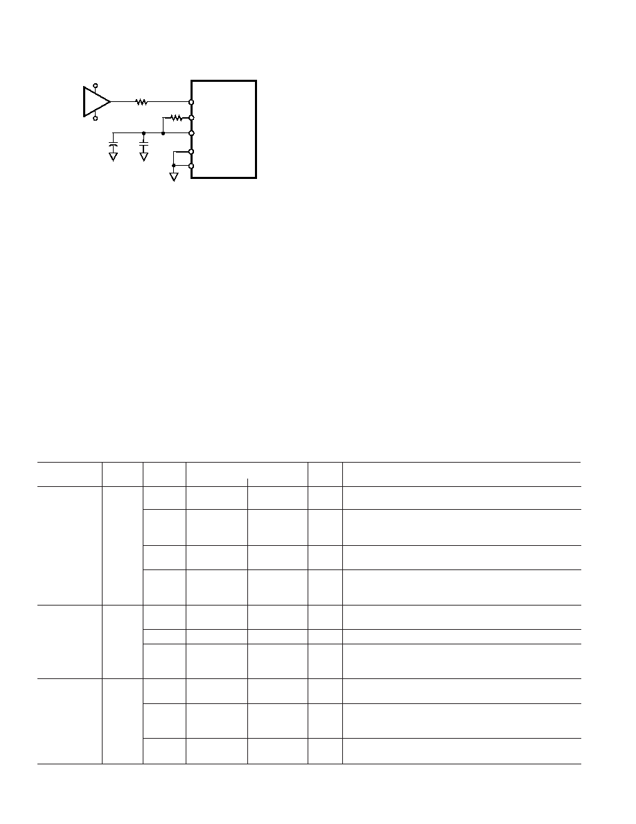
Figure 25. Series Resistor Isolates Switched-Capacitor
SHA Input from Op Amp. Matching Resistors Improve
SNR Performance
The optimum size of this resistor is dependent on several fac-
tors, including the AD9241 sampling rate, the selected op amp
and the particular application. In most applications, a 30
to
50
resistor is sufficient. Some applications may require a
larger resistor value to reduce the noise bandwidth or possibly
limit the fault current in an overvoltage condition. Other appli-
cations may require a larger resistor value as part of an antialiasing
filter. In any case, since the THD performance is dependent on
the series resistance and the above mentioned factors, optimiz-
ing this resistor value for a given application is encouraged.
A slight improvement in SNR performance and dc offset
performance is achieved by matching the input resistance con-
nected to VINA and VINB. The degree of improvement is depen-
dent on the resistor value and the sampling rate. For series
resistor values greater than 100
, the use of a matching
resistor is encouraged.
The noise or small-signal bandwidth of the AD9241 is the same
as its full-power bandwidth. For noise sensitive applications, the
excessive bandwidth may be detrimental and the addition of a
series resistor and/or shunt capacitor can help limit the wide-
band noise at the A/D’s input by forming a low-pass filter. Note,
however, that the combination of this series resistance with the
equivalent input capacitance of the AD9241 should be evalu-
ated for those time-domain applications that are sensitive to the
input signal’s absolute settling time. In applications where har-
monic distortion is not a primary concern, the series resistance
may be selected in combination with the SHA’s nominal 16 pF
of input capacitance to set the filter’s 3 dB cutoff frequency.
A better method of reducing the noise bandwidth, while possi-
bly establishing a real pole for an antialiasing filter, is to add
some additional shunt capacitance between the input (i.e.,
VINA and/or VINB) and analog ground. Since this additional
shunt capacitance combines with the equivalent input capaci-
tance of the AD9241, a lower series resistance can be selected
to establish the filter’s cutoff frequency while not degrading the
distortion performance of the device. The shunt capacitance
also acts as a charge reservoir, sinking or sourcing the additional
charge required by the hold capacitor, CH, further reducing
current transients seen at the op amp’s output.
The effect of this increased capacitive load on the op amp driv-
ing the AD9241 should be evaluated. To optimize performance
when noise is the primary consideration, increase the shunt
capacitance as much as the transient response of the input signal
will allow. Increasing the capacitance too much may adversely
affect the op amp’s settling time, frequency response and distor-
tion performance.
Table I. Analog Input Configuration Summary
Input
Input Range (V)
Figure
Connection
Coupling
Span (V)
VINA
1
VINB
1
#
Comments
Single-Ended
DC
2
0 to 2
1
32, 33
Best for stepped input response applications, suboptimum
THD and noise performance, requires
±5 V op amp.
2
× VREF
0 to
VREF
32, 33
Same as above but with improved noise performance due to
2
× VREF
increase in dynamic range. Headroom/settling time require-
ments of
±5 V op amp should be evaluated.
5
0 to 5
2.5
32, 33
Optimum noise performance, excellent THD performance. Requires
op amp with VCC > +5 V due to insufficient headroom @ 5 V.
2
× VREF
2.5 – VREF
2.5
39
Optimum THD performance with VREF = 1, noise performance
to
improves while THD performance degrades as VREF increases
2.5 + VREF
to 2.5 V. Single supply operation (i.e., +5 V) for many op amps.
Single-Ended
AC
2 or
0 to 1 or
1 or VREF
34
Suboptimum ac performance due to input common-mode
2
× VREF
0 to 2
× VREF
level not biased at optimum midsupply level (i.e., 2.5 V).
5
0 to 5
2.5
34
Optimum noise performance, excellent THD performance.
2
× VREF
2.5 – VREF
2.5
35
Flexible input range, Optimum THD performance with
to
VREF = 1. Noise performance improves while THD performance
2.5 + VREF
degrades as VREF increases to 2.5 V.
Differential
AC or
2
2 to 3
3 to 2
29–31
Optimum full-scale THD and SFDR performance well beyond
DC
the A/Ds Nyquist frequency.
2
× VREF
2.5 – VREF/2
2.5 + VREF/2
29–31
Same as 2 V to 3 V input range with the exception that full-scale
to
THD and SFDR performance can be traded off for better noise
2.5 + VREF/2
2.5 – VREF/2
performance.
5
1.25 to 3.75
3.75 to 1.25
29–31
Widest dynamic range (i.e., ENOBs) due to Optimum Noise
performance.
1VINA and VINB can be interchanged if signal inversion is required.
相关PDF资料 |
PDF描述 |
|---|---|
| MAX9140EUK-T | IC COMPARATOR SGL R-R LP SOT23-5 |
| MAX919EUK/V+T | IC COMPARATOR NANO 1.8V SOT23-5 |
| AD9224ARSZ | IC ADC 12BIT 40MSPS 28-SSOP |
| AD9238BSTZ-40 | IC ADC 12BIT DUAL 40MSPS 64-LQFP |
| VI-J13-MW-F2 | CONVERTER MOD DC/DC 24V 100W |
相关代理商/技术参数 |
参数描述 |
|---|---|
| AD9241ASZRL | 功能描述:IC ADC 14BIT SGL 1.25MSPS 44MQFP RoHS:是 类别:集成电路 (IC) >> 数据采集 - 模数转换器 系列:- 标准包装:1,000 系列:- 位数:12 采样率(每秒):300k 数据接口:并联 转换器数目:1 功率耗散(最大):75mW 电压电源:单电源 工作温度:0°C ~ 70°C 安装类型:表面贴装 封装/外壳:24-SOIC(0.295",7.50mm 宽) 供应商设备封装:24-SOIC 包装:带卷 (TR) 输入数目和类型:1 个单端,单极;1 个单端,双极 |
| AD9241EB | 制造商:AD 制造商全称:Analog Devices 功能描述:Complete 14-Bit, 1.25 MSPS Monolithic A/D Converter |
| AD9241-EB | 制造商:Analog Devices 功能描述:Evaluation Board For AD9241 制造商:Analog Devices 功能描述:EVAL BD FOR AD9241 - Bulk |
| AD9243 | 制造商:AD 制造商全称:Analog Devices 功能描述:Complete 14-Bit, 3.0 MSPS Monolithic A/D Converter |
发布紧急采购,3分钟左右您将得到回复。