- 您现在的位置:买卖IC网 > PDF目录4590 > AD9267BCPZRL7 (Analog Devices Inc)IC MOD SIGMA-DELTA DUAL 64LFCSP PDF资料下载
参数资料
| 型号: | AD9267BCPZRL7 |
| 厂商: | Analog Devices Inc |
| 文件页数: | 11/24页 |
| 文件大小: | 0K |
| 描述: | IC MOD SIGMA-DELTA DUAL 64LFCSP |
| 标准包装: | 750 |
| 类型: | 三角积分调制器 |
| 应用: | 无线通信系统 |
| 安装类型: | 表面贴装 |
| 封装/外壳: | 64-VFQFN 裸露焊盘,CSP |
| 供应商设备封装: | 64-LFCSP-VQ(9x9) |
| 包装: | 带卷 (TR) |
AD9267
Rev. 0 | Page 19 of 24
SERIAL PORT INTERFACE (SPI)
The AD9267 serial port interface (SPI) allows the user to
configure the converter for specific functions or operations
through a structured register space provided inside the ADC.
This provides the user added flexibility and customization
depending on the application. Addresses are accessed via the
serial port and can be written to or read from via the port.
Memory is organized into bytes that are further divided into
fields, as documented in the Memory Map section. For detailed
operational information, see the see the AN-877 Application
Note, Interfacing to High Speed ADCs via SPI.
CONFIGURATION USING THE SPI
As summarized in Table 13, three pins define the SPI of this
ADC. The SCLK pin synchronizes the read and write data
presented to the ADC. The SDIO pin allows data to be sent and
read from the internal ADC memory map registers. The CSB
pin is an active low control that enables or disables the read and
write cycles.
Table 13. Serial Port Interface Pins
Pin
Function
SCLK
SCLK (serial clock) is the serial shift clock. SCLK
synchronizes serial interface reads and writes.
SDIO
SDIO (serial data input/output) is an input and output
depending on the instruction being sent and the
relative position in the timing frame.
CSB
CSB (chip select) is an active low control that gates the
read and write cycles.
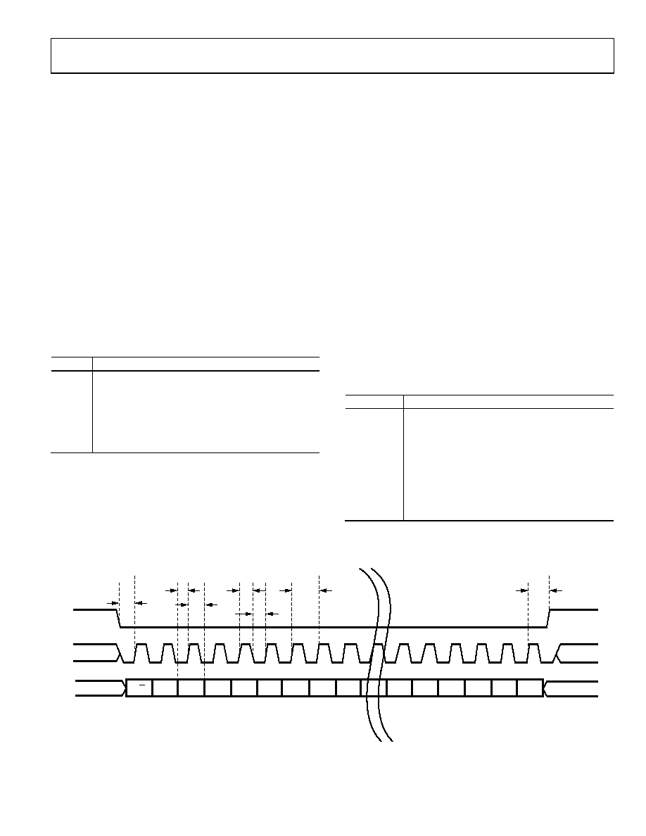
The falling edge of CSB in conjunction with the rising edge of
the SCLK determines the start of the framing. Figure 42 and
Table 14 provide an example of the serial timing and its
definitions.
Other modes involving CSB are available. CSB can be held low
indefinitely to permanently enable the device (this is called
streaming). CSB can stall high between bytes to allow for
additional external timing. When CSB is tied high, SPI
functions are placed in a high impedance mode.
During an instruction phase, a 16-bit instruction is transmitted.
Data follows the instruction phase and the length is determined
by the W0 bit and the W1 bit. All data is composed of 8-bit words.
The first bit of each individual byte of serial data indicates whether
a read or write command is issued. This allows the serial data
input/output (SDIO) pin to change direction from an input to
an output.
In addition to word length, the instruction phase determines if
the serial frame is a read or write operation, allowing the serial
port to be used to both program the chip as well as to read the
contents of the on-chip memory. If the instruction is a readback
operation, performing a readback causes the serial data input/
output (SDIO) pin to change direction from an input to an
output at the appropriate point in the serial frame.
Data can be sent in MSB- or in LSB-first mode. MSB first is
the default setting on power-up and can be changed via the
configuration register. For more information, see the AN-877
Application Note, Interfacing to High Speed ADCs via SPI.
Table 14. SPI Timing Diagram Specifications
Parameter
Definition
tSDS
Setup time between data and rising edge of SCLK
tSDH
Hold time between data and rising edge of SCLK
tSCLK
Period of the clock
tSS
Setup time between CSB and SCLK
tSH
Hold time between CSB and SCLK
tSHIGH
Minimum period that SCLK should be in a logic
high state
tSLOW
Minimum period that SCLK should be in a logic
low state
DON’T CARE
SDIO
SCLK
CSB
tSS
tSDH
tSHIGH
tSCLK
tSLOW
tSDS
tSH
R/W
W1
W0
A12
A11
A10
A9
A8
A7
D5
D4
D3
D2
D1
D0
0
777
3-
03
6
Figure 42. Serial Port Interface Timing Diagram
相关PDF资料 |
PDF描述 |
|---|---|
| LFXP6E-4F256C | IC FPGA 5.8KLUTS 188I/O 256-BGA |
| LFXP6E-3F256I | IC FPGA 5.8KLUTS 188I/O 256-BGA |
| HBC65DRYI | CONN EDGECARD 130PS DIP .100 SLD |
| LFXP6E-4FN256C | IC FPGA 5.8KLUTS 256FPBGA |
| LFXP6E-3FN256I | IC FPGA 5.8KLUTS 188I/O 256-BGA |
相关代理商/技术参数 |
参数描述 |
|---|---|
| AD9267EBZ | 功能描述:BOARD EVALUATION FOR AD9267 RoHS:是 类别:编程器,开发系统 >> 评估板 - 模数转换器 (ADC) 系列:- 产品培训模块:Obsolescence Mitigation Program 标准包装:1 系列:- ADC 的数量:1 位数:12 采样率(每秒):94.4k 数据接口:USB 输入范围:±VREF/2 在以下条件下的电源(标准):- 工作温度:-40°C ~ 85°C 已用 IC / 零件:MAX11645 已供物品:板,软件 |
| AD9268 | 制造商:AD 制造商全称:Analog Devices 功能描述:16-Bit, 80 MSPS/105 MSPS/125 MSPS, 1.8 V Dual Analog-to-Digital Converter (ADC) |
| AD9268-105EBZ1 | 制造商:AD 制造商全称:Analog Devices 功能描述:16-Bit, 80 MSPS/105 MSPS/125 MSPS, 1.8 V Dual Analog-to-Digital Converter (ADC) |
| AD9268-125EBZ | 功能描述:数据转换 IC 开发工具 Dual 16 bit 125 high SNR ADC RoHS:否 制造商:Texas Instruments 产品:Demonstration Kits 类型:ADC 工具用于评估:ADS130E08 接口类型:SPI 工作电源电压:- 6 V to + 6 V |
| AD9268-125EBZ1 | 制造商:AD 制造商全称:Analog Devices 功能描述:16-Bit, 80 MSPS/105 MSPS/125 MSPS, 1.8 V Dual Analog-to-Digital Converter (ADC) |
发布紧急采购,3分钟左右您将得到回复。