- 您现在的位置:买卖IC网 > PDF目录4590 > AD9267BCPZRL7 (Analog Devices Inc)IC MOD SIGMA-DELTA DUAL 64LFCSP PDF资料下载
参数资料
| 型号: | AD9267BCPZRL7 |
| 厂商: | Analog Devices Inc |
| 文件页数: | 14/24页 |
| 文件大小: | 0K |
| 描述: | IC MOD SIGMA-DELTA DUAL 64LFCSP |
| 标准包装: | 750 |
| 类型: | 三角积分调制器 |
| 应用: | 无线通信系统 |
| 安装类型: | 表面贴装 |
| 封装/外壳: | 64-VFQFN 裸露焊盘,CSP |
| 供应商设备封装: | 64-LFCSP-VQ(9x9) |
| 包装: | 带卷 (TR) |
AD9267
Rev. 0 | Page 21 of 24
APPLICATIONS INFORMATION
FILTERING REQUIREMENT
The need for anti-alias protection often requires one or two
octaves for a transition band, which reduces the usable
bandwidth of a Nyquist converter to between 25% and 50% of
the available bandwidth. A CT Σ-Δ converter maximizes the
available signal bandwidth by forgoing the need for an
antialiasing filter because the architecture possesses inherent
antialiasing. Although a high order, sharp cutoff antialiasing
filter may not be necessary because of the unique characteristics
of the architecture, a low order filter may still be required to
precede the ADC for out-of-band signal handling.
Depending on the application and the system architecture, this
low order filter may or may not be necessary. The signal
transfer function (STF) of a continuous time feedforward ADC
usually contains out-of-band peaks. Because these STF peaks
are typically one or two octaves above the pass-band edge, they
are not problematic in applications where the bulk of the signal
energy is in or near the pass band. However, in applications
with large far-out interferers, it is necessary to either add a filter
to attenuate these problematic signals or to allocate some of the
ADC dynamic range to accommodate them.
Figure 43 shows the normalized STF of the AD9267 CT Σ-Δ
converter. The figure shows out-of-band peaking beyond the
band edge of the ADC. Within the 10 MHz band of interest, the
STF is maximally flat with less than 0.1 dB of gain. Maximum
peaking occurs at 60 MHz with 10 dB of gain. To put this into
perspective, for a fixed input power, a 5 MHz in-band-signal
appears at 5 dBFS, a 25 MHz tone appears at 2 dBFS and
60 MHz tone at +5 dBFS. Because the maximum input to the
ADC is 2 dBFS, large out-of-band signals can quickly saturate
the system. This implies that under these conditions, the digital
outputs of the ADC no longer accurately represents the input.
Refer to the Overrange (OR) Condition section for details on
overrange detection and recovery.
15
13
11
9
7
5
3
1
–1
–3
–5
0
1020
3040
5060
708090
100
FREQUENCY (MHz)
GA
IN
(
d
B
)
07
77
3-
0
49
Figure 43. STF
Figure 43 shows the gain profile of the AD9267 and this can be
interpreted as the level in which the signal power should be
scaled back to prevent an overload condition. This is the
ultimate trip point and before this point is reached, the in-band
noise (IBN) slowly degrades. As a result, it is recommended that
the low-pass filter be designed to match the profile of Figure 44,
which shows the maximum input signal for a 3 dB degradation
of in-band noise. The input signal is attenuated to allow only
3 dB of noise degradation over frequency.
The noise performance is normalized to a 2 dBFS in-band
signal. The AD9267 STF and NTF are flat within the band of
interest and should result in almost no change in input level and
IBN. Beyond the bandwidth of the AD9267, out-of-band
peaking adds gain to the system, therefore requiring the input
power to be scaled back to prevent in-band noise degradation.
The input power is scaled back to a point where only 3 dB of
noise degradation is allowed, therefore resulting in Figure 44.
5
0
–5
–10
–15
–20
–25
0
10
2030
405060
7080
90
100
FREQUENCY (MHz)
AM
P
L
IT
UD
E
(
d
B)
CHEBYSHEV II
FILTER RESPONSE
–40°C
+85°C
+25°C
07
77
3-
05
1
Figure 44. Maximum Input Level for 3 dB Noise Degradation
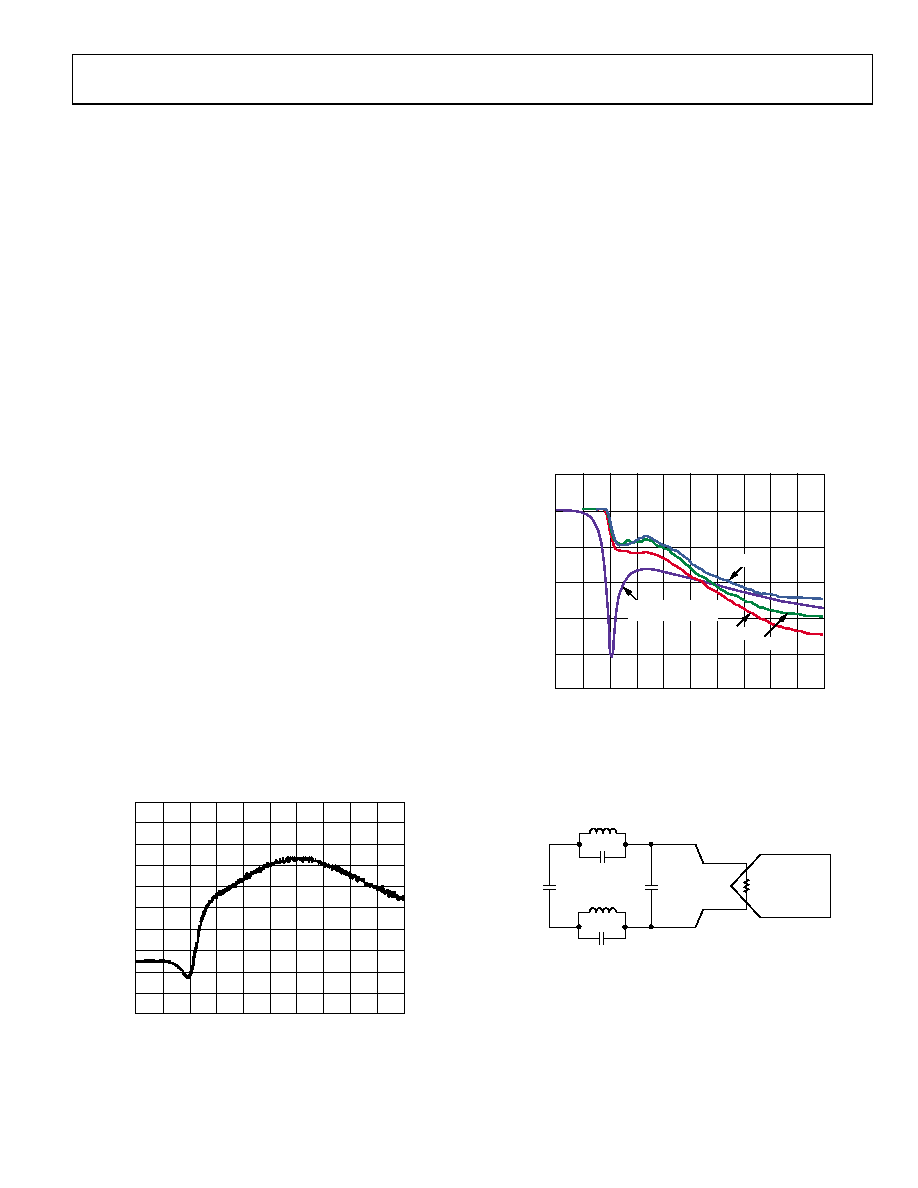
An example third-order low-pass Chebyshev II type filter is
shown in Figure 45 and the corresponding magnitude vs.
frequency response of the filter is shown in Figure 44.
07
773
-05
2
L1
180nH
L1
180nH
C2
390pF
C2
390pF
C3
220pF
C1
39pF
1k
AD9267
CT
Σ-Δ
VIN+
VIN–
Figure 45. Third-Order Low-Pass Chebyshev II Filter
相关PDF资料 |
PDF描述 |
|---|---|
| LFXP6E-4F256C | IC FPGA 5.8KLUTS 188I/O 256-BGA |
| LFXP6E-3F256I | IC FPGA 5.8KLUTS 188I/O 256-BGA |
| HBC65DRYI | CONN EDGECARD 130PS DIP .100 SLD |
| LFXP6E-4FN256C | IC FPGA 5.8KLUTS 256FPBGA |
| LFXP6E-3FN256I | IC FPGA 5.8KLUTS 188I/O 256-BGA |
相关代理商/技术参数 |
参数描述 |
|---|---|
| AD9267EBZ | 功能描述:BOARD EVALUATION FOR AD9267 RoHS:是 类别:编程器,开发系统 >> 评估板 - 模数转换器 (ADC) 系列:- 产品培训模块:Obsolescence Mitigation Program 标准包装:1 系列:- ADC 的数量:1 位数:12 采样率(每秒):94.4k 数据接口:USB 输入范围:±VREF/2 在以下条件下的电源(标准):- 工作温度:-40°C ~ 85°C 已用 IC / 零件:MAX11645 已供物品:板,软件 |
| AD9268 | 制造商:AD 制造商全称:Analog Devices 功能描述:16-Bit, 80 MSPS/105 MSPS/125 MSPS, 1.8 V Dual Analog-to-Digital Converter (ADC) |
| AD9268-105EBZ1 | 制造商:AD 制造商全称:Analog Devices 功能描述:16-Bit, 80 MSPS/105 MSPS/125 MSPS, 1.8 V Dual Analog-to-Digital Converter (ADC) |
| AD9268-125EBZ | 功能描述:数据转换 IC 开发工具 Dual 16 bit 125 high SNR ADC RoHS:否 制造商:Texas Instruments 产品:Demonstration Kits 类型:ADC 工具用于评估:ADS130E08 接口类型:SPI 工作电源电压:- 6 V to + 6 V |
| AD9268-125EBZ1 | 制造商:AD 制造商全称:Analog Devices 功能描述:16-Bit, 80 MSPS/105 MSPS/125 MSPS, 1.8 V Dual Analog-to-Digital Converter (ADC) |
发布紧急采购,3分钟左右您将得到回复。