- 您现在的位置:买卖IC网 > PDF目录4590 > AD9267BCPZRL7 (Analog Devices Inc)IC MOD SIGMA-DELTA DUAL 64LFCSP PDF资料下载
参数资料
| 型号: | AD9267BCPZRL7 |
| 厂商: | Analog Devices Inc |
| 文件页数: | 7/24页 |
| 文件大小: | 0K |
| 描述: | IC MOD SIGMA-DELTA DUAL 64LFCSP |
| 标准包装: | 750 |
| 类型: | 三角积分调制器 |
| 应用: | 无线通信系统 |
| 安装类型: | 表面贴装 |
| 封装/外壳: | 64-VFQFN 裸露焊盘,CSP |
| 供应商设备封装: | 64-LFCSP-VQ(9x9) |
| 包装: | 带卷 (TR) |
AD9267
Rev. 0 | Page 15 of 24
The second mode bypasses the clock multiplier circuitry and
allows the clock to be directly sourced. This mode enables the
user to source a very high quality clock directly to the Σ-Δ
modulator. Sourcing the clock directly may be necessary in
demanding applications that require the lowest possible output
noise. Refer to Figure 18, which shows the degradation in SNR
performance for the various PLL settings.
In either case, when using the on-chip clock multiplier or
sourcing the high speed clock directly, it is necessary that the
clock source have low jitter to maximize the Σ-Δ modulator
noise performance. High speed, high resolution ADCs and
modulators are sensitive to the quality of the clock input. As
jitter increases, the SNR performance of the AD9267 degrades
from that specified in Table 2. The jitter inherent to the part due
to the PLL root sum squares with any external clock jitter,
thereby degrading performance. To prevent jitter from dominating
the performance of the AD9267, the input clock source should be
no greater than 1 ps rms of jitter.
The CLK± inputs are self-biased to 450 mV (see Figure 21); if
dc-coupled, it is important to maintain the specified 450 mV
input common-mode voltage. Each input pin can safely swing
from 200 mV p-p to 1 V p-p single-ended about the 450 mV
common-mode voltage. The recommended clock inputs are
CMOS or LVPECL.
The specified clock rate of the Σ-Δ modulator, fMOD, is 640 MHz.
The clock rate possesses a direct relationship with the available
input bandwidth of the ADC.
Bandwidth = fMOD ÷ 64
In either case, using the on-chip clock multiplier to generate the
Σ-Δ modulator clock rate or directly sourcing the clock, any
deviation from 640 MHz results in a change in input bandwidth.
The input range of the clock is limited to 640 MHz ± 5%.
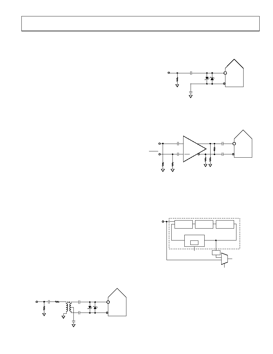
Direct Clocking
The default configuration of the AD9267 is for direct clocking
where the PLL is bypassed. Figure 38 shows one preferred
method for clocking the AD9267. A low jitter clock source is
converted from a single-ended signal to a differential signal
using an RF transformer. The back-to-back Schottky diodes
across the secondary side of the transformer limits clock
excursions into the AD9267 to approximately 0.8 V p-p differen-
tial. This helps prevent the large voltage swings of the clock
from feeding through to other portions of the AD9267 while
preserving the fast rise and fall times of the signal, which are
critical to achieving low jitter.
CLOCK
INPUT
XFMR
MINI-CIRCUITS
TC1-1-13M+, 1:1
SCHOTTKY
DIODES:
HSM2812
50
CLK+
CLK–
0.1F
ADC
AD9267
0.1F
0
77
73
-0
53
Figure 38. Transformer-Coupled Differential Clock
If a differential clock is not available, the AD9267 can be driven
by a single-ended signal into the CLK+ terminal with the CLK
terminal ac-coupled to ground. Figure 39 shows the circuit
configuration.
SCHOTTKY
DIODES:
HSM2812
50
CLK+
CLK–
0.1F
ADC
AD9267
CLOCK
INPUT
0
77
73
-05
4
Figure 39. Single-Ended Clock
Another option is to ac couple a differential LVPECL signal to
the sample clock input pins, as shown in Figure 40. The AD951x
family of clock drivers is recommended because it offers excellent
jitter performance.
100
240
240
50
1
150
RESISTORS ARE OPTIONAL.
50
1
CLK+
CLK–
0.1F
ADC
AD9267
CLOCK
INPUT
CLOCK
INPUT
0.1F
CLK
AD951x
LVPECL
DRIVER
CLK
0
7773-
05
5
Figure 40. Differential LVPECL Sample Clock
Internal PLL Clock Distribution
The alternative clocking option available on the AD9267 is to
apply a low frequency reference clock and use the on-chip clock
multiplier to generate the high frequency fMOD rate. The internal
clock architecture is shown in Figure 41.
PHASE
DETECTOR
DIVIDER
PLLMULT
0x0A[5:0]
CLK±
MODULATOR
CLOCK
640MSPS
PLLENABLE
0x09[2]
÷N
LOOP
FILTER
VCO
PLL
÷2
07
77
3-
04
0
Figure 41. Internal Clock Architecture
The clock multiplication circuit operates such that the VCO
outputs a frequency, fVCO, equal to the reference clock input
multiplied by N
fVCO = (CLK±) × (N)
where N is the PLL multiplication (PLLMULT) factor.
The Σ-Δ modulator clock frequency, fMOD, is equal to
fMOD = fVCO ÷ 2
相关PDF资料 |
PDF描述 |
|---|---|
| LFXP6E-4F256C | IC FPGA 5.8KLUTS 188I/O 256-BGA |
| LFXP6E-3F256I | IC FPGA 5.8KLUTS 188I/O 256-BGA |
| HBC65DRYI | CONN EDGECARD 130PS DIP .100 SLD |
| LFXP6E-4FN256C | IC FPGA 5.8KLUTS 256FPBGA |
| LFXP6E-3FN256I | IC FPGA 5.8KLUTS 188I/O 256-BGA |
相关代理商/技术参数 |
参数描述 |
|---|---|
| AD9267EBZ | 功能描述:BOARD EVALUATION FOR AD9267 RoHS:是 类别:编程器,开发系统 >> 评估板 - 模数转换器 (ADC) 系列:- 产品培训模块:Obsolescence Mitigation Program 标准包装:1 系列:- ADC 的数量:1 位数:12 采样率(每秒):94.4k 数据接口:USB 输入范围:±VREF/2 在以下条件下的电源(标准):- 工作温度:-40°C ~ 85°C 已用 IC / 零件:MAX11645 已供物品:板,软件 |
| AD9268 | 制造商:AD 制造商全称:Analog Devices 功能描述:16-Bit, 80 MSPS/105 MSPS/125 MSPS, 1.8 V Dual Analog-to-Digital Converter (ADC) |
| AD9268-105EBZ1 | 制造商:AD 制造商全称:Analog Devices 功能描述:16-Bit, 80 MSPS/105 MSPS/125 MSPS, 1.8 V Dual Analog-to-Digital Converter (ADC) |
| AD9268-125EBZ | 功能描述:数据转换 IC 开发工具 Dual 16 bit 125 high SNR ADC RoHS:否 制造商:Texas Instruments 产品:Demonstration Kits 类型:ADC 工具用于评估:ADS130E08 接口类型:SPI 工作电源电压:- 6 V to + 6 V |
| AD9268-125EBZ1 | 制造商:AD 制造商全称:Analog Devices 功能描述:16-Bit, 80 MSPS/105 MSPS/125 MSPS, 1.8 V Dual Analog-to-Digital Converter (ADC) |
发布紧急采购,3分钟左右您将得到回复。