- 您现在的位置:买卖IC网 > PDF目录10516 > AD9286BCPZ-500 (Analog Devices Inc)IC ADC 8BIT SPI/SRL 500M 48LFSCP PDF资料下载
参数资料
| 型号: | AD9286BCPZ-500 |
| 厂商: | Analog Devices Inc |
| 文件页数: | 2/28页 |
| 文件大小: | 0K |
| 描述: | IC ADC 8BIT SPI/SRL 500M 48LFSCP |
| 标准包装: | 1 |
| 位数: | 8 |
| 采样率(每秒): | 500M |
| 数据接口: | 串行,SPI? |
| 转换器数目: | 2 |
| 功率耗散(最大): | 330mW |
| 电压电源: | 模拟和数字 |
| 工作温度: | -40°C ~ 85°C |
| 安装类型: | 表面贴装 |
| 封装/外壳: | 48-VFQFN 裸露焊盘,CSP |
| 供应商设备封装: | 48-LFCSP-VQ(7x7) |
| 包装: | 托盘 |
| 输入数目和类型: | 2 个差分,双极 |
第1页当前第2页第3页第4页第5页第6页第7页第8页第9页第10页第11页第12页第13页第14页第15页第16页第17页第18页第19页第20页第21页第22页第23页第24页第25页第26页第27页第28页
AD9286
Data Sheet
Rev. B | Page 10 of 28
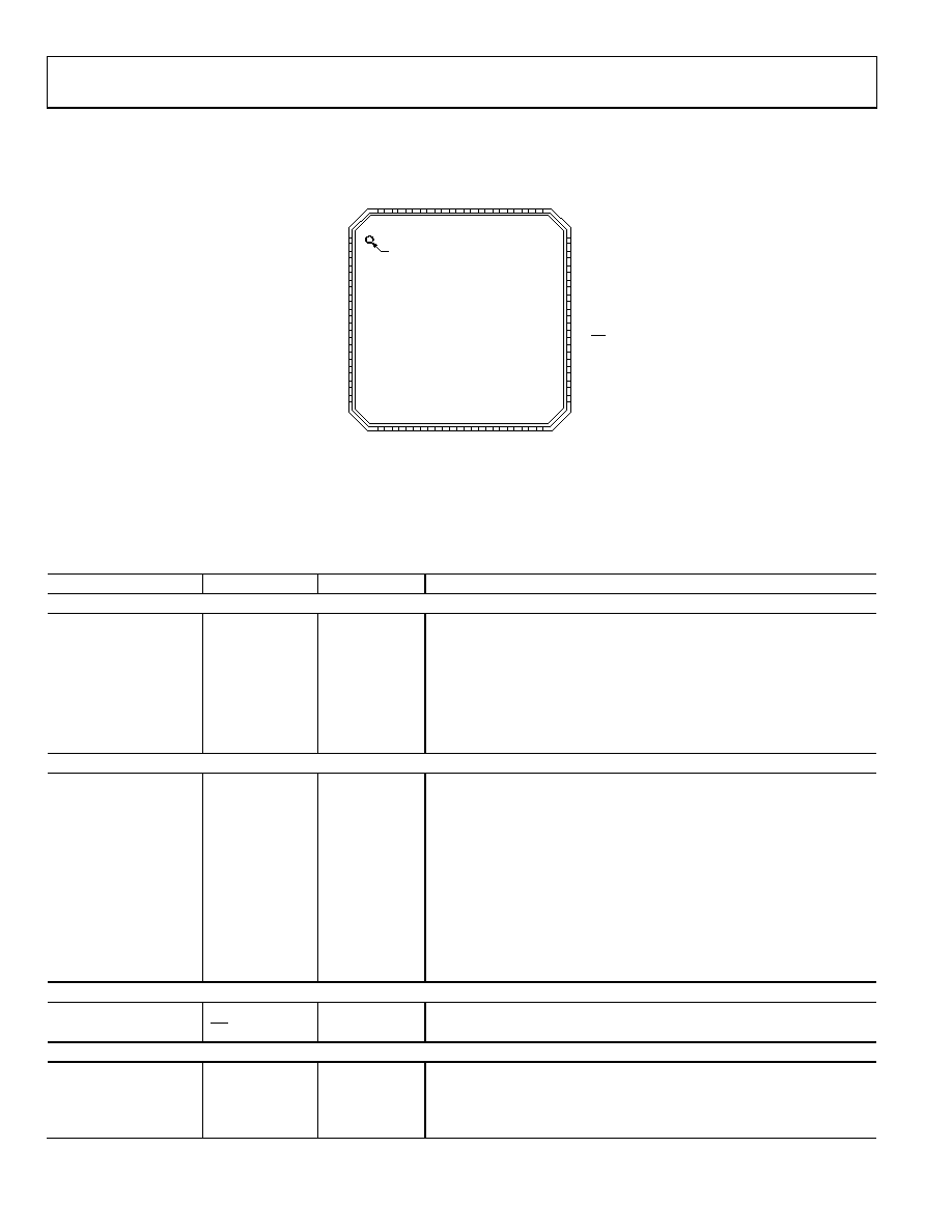
PIN CONFIGURATION AND FUNCTION DESCRIPTIONS
09338-
003
13
14
15
16
17
18
19
20
21
22
23
24
D2–
D2+
D3–
D3+
DCO
–
DCO
+
D4–
D4+
D5–
D5+
D6–
D6+
48
47
46
45
44
43
42
41
40
39
38
37
AV
DD
V
IN2–
V
IN2+
AV
DD
AV
DD
VR
EF
AV
DD
V
CM
AV
DD
V
IN1+
V
IN1–
AV
DD
1
2
3
4
5
6
7
8
9
10
11
12
AVDD
AUXCLK+
AUXCLK–
RBIAS
AUXCLKEN
DRGND
DRVDD
D0– (LSB)
D0+ (LSB)
D1–
D1+
AVDD
CLK+
CLK–
CSB
SDIO/PWDN
SCLK
OE
DRGND
DRVDD
D7+ (MSB)
D7– (MSB)
35
AVDD
36
34
33
32
31
30
29
28
27
26
25
AD9286
TOP VIEW
(Not to Scale)
PIN 1
INDICATOR
NOTES
1. THE EXPOSED PADDLE MUST BE SOLDERED TO THE PCB ANALOG
GROUND TO ENSURE PROPER FUNCTIONALITY AND HEAT
DISSIPATION, NOISE, AND MECHANICAL STRENGTH BENEFITS.
Figure 6. Pin Configuration
Table 8. Pin Function Descriptions
Pin No.
Mnemonic
Type
Description
ADC Power Pins
1, 2, 35, 36, 37, 40, 42,
44, 45, 48
AVDD
Supply
Analog Power Supply (1.8 V Nominal).
8, 27
DRVDD
Supply
Digital Output Driver Supply (1.8 V Nominal).
7, 28
DRGND
Ground
Digital Output Ground.
0
AGND
Ground
Analog Ground. Pin 0 is the exposed thermal pad on the bottom of the
package. This is the only ground connection, and it must be soldered to
the PCB analog ground to ensure proper functionality and heat dissipation,
noise, and mechanical strength benefits.
ADC Analog Pins
39
VIN1+
Input
Differential Analog Input Pin (+) for Channel 1.
38
VIN1
Input
Differential Analog Input Pin () for Channel 1.
46
VIN2+
Input
Differential Analog Input Pin (+) for Channel 2.
47
VIN2
Input
Differential Analog Input Pin () for Channel 2.
43
VREF
Input/output
Voltage Reference Input/Output.
5
RBIAS
Input/output
External Reference Bias Resistor. Connect 10 kΩ from RBIAS to AGND.
41
VCM
Output
Common-Mode Level Bias Output for Analog Inputs.
34
CLK+
Input
ADC Clock Input—True.
33
CLK
Input
ADC Clock Input—Complement.
3
AUXCLK+
Input
Auxiliary ADC Clock Input—True.
4
AUXCLK
Input
Auxiliary ADC Clock Input—Complement.
Digital Inputs
6
AUXCLKEN
Input
Auxiliary Clock Input Enable.
29
OE
Input
Digital Enable (Active Low) to Tristate Output Data Pins.
Digital Outputs
26
D7+ (MSB)
Output
Output Data 7—True.
25
D7 (MSB)
Output
Output Data 7—Complement.
24
D6+
Output
Output Data 6—True.
23
D6
Output
Output Data 6—Complement.
相关PDF资料 |
PDF描述 |
|---|---|
| UP050B821K-KFC | CAP CER 820PF 50V 10% AXIAL |
| VE-B4B-MX-F3 | CONVERTER MOD DC/DC 95V 75W |
| MAX3450EEUD+ | TXRX USB +/-15KV ESD 14-TSSOP |
| VE-B4B-MX-F1 | CONVERTER MOD DC/DC 95V 75W |
| AD976ABNZ | IC ADC 16BIT 200KSPS 28-DIP |
相关代理商/技术参数 |
参数描述 |
|---|---|
| AD9286BCPZRL7-500 | 功能描述:IC ADC 8BIT SPI/SRL 500M 48LFCSP RoHS:是 类别:集成电路 (IC) >> 数据采集 - 模数转换器 系列:- 标准包装:1 系列:- 位数:14 采样率(每秒):83k 数据接口:串行,并联 转换器数目:1 功率耗散(最大):95mW 电压电源:双 ± 工作温度:0°C ~ 70°C 安装类型:通孔 封装/外壳:28-DIP(0.600",15.24mm) 供应商设备封装:28-PDIP 包装:管件 输入数目和类型:1 个单端,双极 |
| AD9287 | 制造商:AD 制造商全称:Analog Devices 功能描述:Quad, 8-Bit, 100 MSPS Serial LVDS 1.8 V A/D Converter |
| AD9287-100EB | 制造商:Analog Devices 功能描述: |
| AD9287-100EB1 | 制造商:AD 制造商全称:Analog Devices 功能描述:High Speed ADC USB FIFO Evaluation Kit |
| AD9287-100EBZ | 功能描述:BOARD EVALUATION AD9287 RoHS:是 类别:编程器,开发系统 >> 评估板 - 模数转换器 (ADC) 系列:- 产品培训模块:Obsolescence Mitigation Program 标准包装:1 系列:- ADC 的数量:1 位数:12 采样率(每秒):94.4k 数据接口:USB 输入范围:±VREF/2 在以下条件下的电源(标准):- 工作温度:-40°C ~ 85°C 已用 IC / 零件:MAX11645 已供物品:板,软件 |
发布紧急采购,3分钟左右您将得到回复。