- 您现在的位置:买卖IC网 > PDF目录10516 > AD9286BCPZ-500 (Analog Devices Inc)IC ADC 8BIT SPI/SRL 500M 48LFSCP PDF资料下载
参数资料
| 型号: | AD9286BCPZ-500 |
| 厂商: | Analog Devices Inc |
| 文件页数: | 7/28页 |
| 文件大小: | 0K |
| 描述: | IC ADC 8BIT SPI/SRL 500M 48LFSCP |
| 标准包装: | 1 |
| 位数: | 8 |
| 采样率(每秒): | 500M |
| 数据接口: | 串行,SPI? |
| 转换器数目: | 2 |
| 功率耗散(最大): | 330mW |
| 电压电源: | 模拟和数字 |
| 工作温度: | -40°C ~ 85°C |
| 安装类型: | 表面贴装 |
| 封装/外壳: | 48-VFQFN 裸露焊盘,CSP |
| 供应商设备封装: | 48-LFCSP-VQ(7x7) |
| 包装: | 托盘 |
| 输入数目和类型: | 2 个差分,双极 |
第1页第2页第3页第4页第5页第6页当前第7页第8页第9页第10页第11页第12页第13页第14页第15页第16页第17页第18页第19页第20页第21页第22页第23页第24页第25页第26页第27页第28页
Data Sheet
AD9286
Rev. B | Page 15 of 28
THEORY OF OPERATION
The AD9286 is a pipeline-type converter. The input buffers are
differential, and both sets of inputs are internally biased. This
allows the use of ac or dc input modes. A sample-and-hold
amplifier is incorporated into the first stage of the multistage
pipeline converter core. The output staging block aligns the data,
carries out error correction for the pipeline stages, and feeds
that data to the output interleave block and, finally, to the output
buffers. All user-selected options are programmed through
dedicated digital input pins or a serial port interface (SPI).
ADC ARCHITECTURE
Each interleaving channel of the AD9286 consists of a differential
input buffer followed by a sample-and-hold amplifier (SHA).
This SHA is followed by a pipeline switched-capacitor ADC.
The quantized outputs from each stage are combined into a final
8-bit result in the digital correction logic. The pipelined archi-
tecture permits the first stage to operate on a new input sample,
whereas the remaining stages operate on preceding samples.
Each stage of the pipeline, excluding the last, consists of a low
resolution flash ADC connected to a switched-capacitor DAC
and interstage residue amplifier (MDAC). The residue amplifier
magnifies the difference between the reconstructed DAC output
and the flash input for the next stage in the pipeline. One bit of
redundancy is used in each stage to facilitate digital correction
of flash errors. The last stage consists of a flash ADC.
The input stage contains a differential SHA that can be ac- or
dc-coupled in differential or single-ended mode. The output
staging block aligns the data, carries out the error correction,
and passes the data to the output buffers. The output buffers
are powered from a separate supply, allowing adjustment of the
output voltage swing. During power-down, the output buffers
go into a high impedance state.
The outputs from both interleaving channels are time interleaved
to achieve an effective 500 MSPS.
ANALOG INPUT CONSIDERATIONS
The analog inputs of the AD9286 are differentially buffered.
For best dynamic performance, the source impedances driving
VIN1+, VIN1, VIN2+, and VIN2 should be matched such
that common-mode settling errors are symmetrical. Because
the AD9286 interleaves two ADC cores, special attention should
be given, during board layout, to the symmetry of the two analog
paths. Mismatch introduces undesired distortion. The analog
inputs are optimized to provide superior wideband performance
and must be driven differentially. SNR and SINAD performance
degrades significantly if the analog inputs are driven with
a single-ended signal.
A wideband transformer, such as Mini-Circuits ADT1-1WT, can
provide the differential analog inputs for applications that require
a single-ended-to-differential conversion. Both analog inputs
are self-biased by an on-chip resistor divider to a nominal 1.4 V.
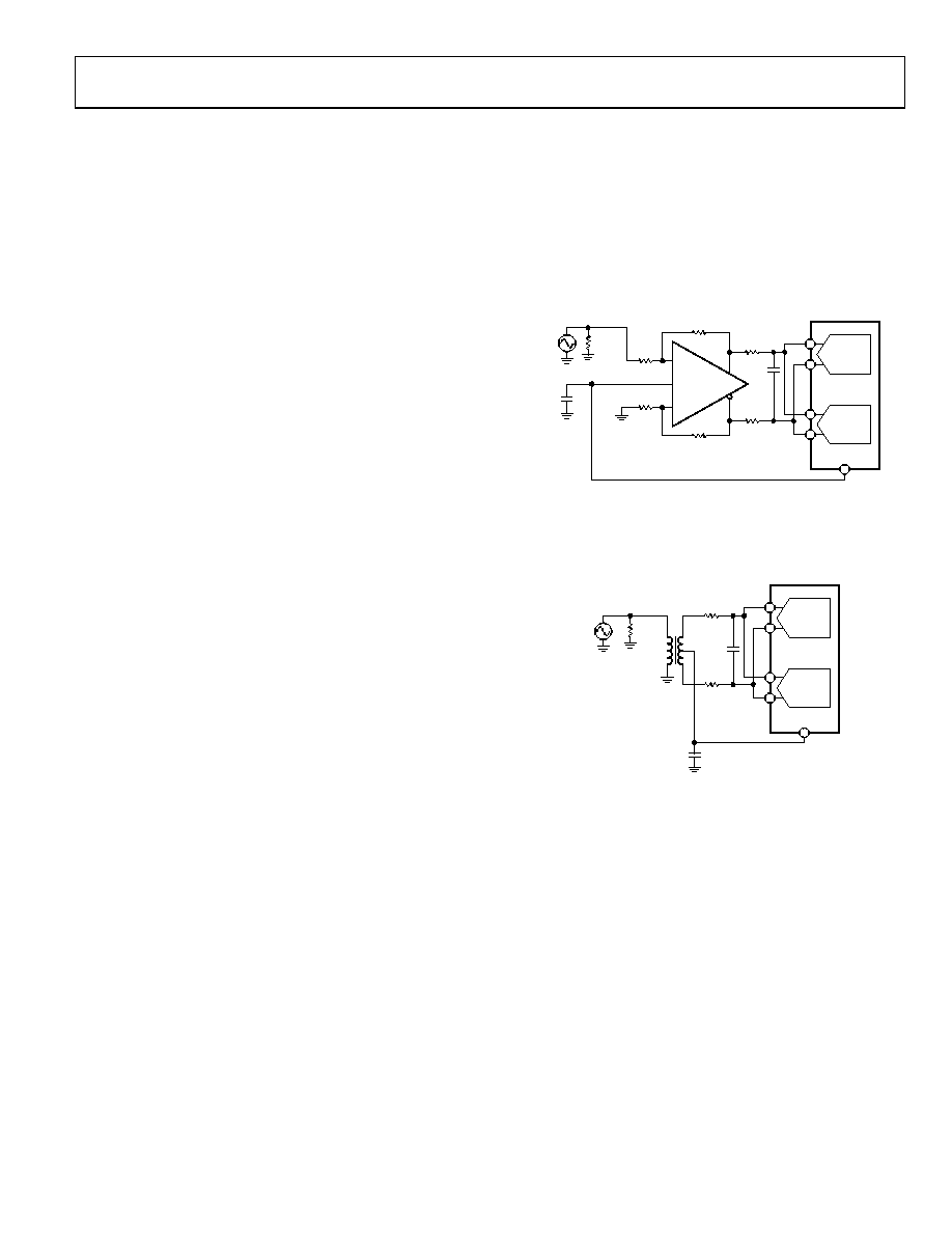
Differential Input Configurations
Optimum performance is achieved when driving the AD9286
in a differential input configuration. For baseband applications,
the ADA4937-1 differential driver provides excellent performance
and a flexible interface to the ADC (see Figure 24). The output
common-mode voltage of the AD9286 is easily set to 1.4 V, and
the driver can be configured in a Sallen-Key filter topology to
provide band limiting of the input signal.
–
+
200
227.4
61.9
ADA4937-1
1.2V p-p
0.1F
200
VIN1
VIN2
+
–
+
–
4.7pF
33
AD9286
VCM
09338-
025
Figure 24. Differential Input Configuration Using the ADA4937-1
The AD9286 can also be driven passively with a differential
transformer-coupled input (see Figure 25). To bias the analog
input, the VCM voltage can be connected to the center tap of
the secondary winding of the transformer.
49.9
1.2V p-p
VIN1
VIN2
+
–
+
–
4.7pF
0.1F
33
AD9286
VCM
09338-
026
Figure 25. Differential Transformer-Coupled Configuration
The signal characteristics must be considered when selecting a
transformer. Most RF transformers saturate at frequencies below
a few megahertz (MHz). Excessive signal power can also cause
core saturation, which leads to distortion.
VOLTAGE REFERENCE
An internal differential voltage reference creates positive and
negative reference voltages that define the 1.2 V p-p fixed span
of the ADC core. This internal voltage reference can be adjusted
by means of SPI control. It can also be driven externally with
an off-chip stable reference. See the Memory Map Register
Descriptions section for more details.
RBIAS
The AD9286 requires the user to place a 10 kΩ resistor between
the RBIAS pin and ground. This resistor, which is used to set
the master current reference of the ADC core, should have a 1%
tolerance.
相关PDF资料 |
PDF描述 |
|---|---|
| UP050B821K-KFC | CAP CER 820PF 50V 10% AXIAL |
| VE-B4B-MX-F3 | CONVERTER MOD DC/DC 95V 75W |
| MAX3450EEUD+ | TXRX USB +/-15KV ESD 14-TSSOP |
| VE-B4B-MX-F1 | CONVERTER MOD DC/DC 95V 75W |
| AD976ABNZ | IC ADC 16BIT 200KSPS 28-DIP |
相关代理商/技术参数 |
参数描述 |
|---|---|
| AD9286BCPZRL7-500 | 功能描述:IC ADC 8BIT SPI/SRL 500M 48LFCSP RoHS:是 类别:集成电路 (IC) >> 数据采集 - 模数转换器 系列:- 标准包装:1 系列:- 位数:14 采样率(每秒):83k 数据接口:串行,并联 转换器数目:1 功率耗散(最大):95mW 电压电源:双 ± 工作温度:0°C ~ 70°C 安装类型:通孔 封装/外壳:28-DIP(0.600",15.24mm) 供应商设备封装:28-PDIP 包装:管件 输入数目和类型:1 个单端,双极 |
| AD9287 | 制造商:AD 制造商全称:Analog Devices 功能描述:Quad, 8-Bit, 100 MSPS Serial LVDS 1.8 V A/D Converter |
| AD9287-100EB | 制造商:Analog Devices 功能描述: |
| AD9287-100EB1 | 制造商:AD 制造商全称:Analog Devices 功能描述:High Speed ADC USB FIFO Evaluation Kit |
| AD9287-100EBZ | 功能描述:BOARD EVALUATION AD9287 RoHS:是 类别:编程器,开发系统 >> 评估板 - 模数转换器 (ADC) 系列:- 产品培训模块:Obsolescence Mitigation Program 标准包装:1 系列:- ADC 的数量:1 位数:12 采样率(每秒):94.4k 数据接口:USB 输入范围:±VREF/2 在以下条件下的电源(标准):- 工作温度:-40°C ~ 85°C 已用 IC / 零件:MAX11645 已供物品:板,软件 |
发布紧急采购,3分钟左右您将得到回复。