参数资料
| 型号: | AD9444BSVZ-80 |
| 厂商: | Analog Devices Inc |
| 文件页数: | 13/40页 |
| 文件大小: | 0K |
| 描述: | IC ADC 14BIT 80MSPS 100TQFP |
| 标准包装: | 1 |
| 位数: | 14 |
| 采样率(每秒): | 80M |
| 数据接口: | 并联 |
| 转换器数目: | 1 |
| 功率耗散(最大): | 1.4W |
| 电压电源: | 单电源 |
| 工作温度: | -40°C ~ 85°C |
| 安装类型: | 表面贴装 |
| 封装/外壳: | 100-TQFP 裸露焊盘 |
| 供应商设备封装: | 100-TQFP-EP(14x14) |
| 包装: | 托盘 |
| 输入数目和类型: | 1 个差分,单极 |
第1页第2页第3页第4页第5页第6页第7页第8页第9页第10页第11页第12页当前第13页第14页第15页第16页第17页第18页第19页第20页第21页第22页第23页第24页第25页第26页第27页第28页第29页第30页第31页第32页第33页第34页第35页第36页第37页第38页第39页第40页
AD9444
Rev. 0 | Page 20 of 40
THEORY OF OPERATION
The AD9444 architecture is optimized for high speed and ease
of use. The analog inputs drive an integrated, high bandwidth,
track-and-hold circuit that samples the signal prior to quantiza-
tion by the 14-bit pipeline ADC core. The device includes an
on-board reference and input logic that accepts TTL, CMOS, or
LVPECL levels. The digital output logic levels are user selectable
as standard 3 V CMOS or LVDS (ANSI-644 compatible) via the
OUTPUT MODE pin.
ANALOG INPUT AND REFERENCE OVERVIEW
A stable and accurate 0.5 V voltage reference is built into the
AD9444. The input range can be adjusted by varying the refer-
ence voltage applied to the AD9444, using either the internal
reference or an externally applied reference voltage. The input
span of the ADC tracks reference voltage changes linearly. The
various reference modes are described in the next few sections.
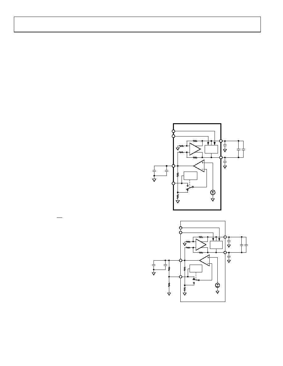
Internal Reference Connection
A comparator within the AD9444 detects the potential at the
SENSE pin and configures the reference into four possible
states, which are summarized in Table 9. If SENSE is grounded,
the reference amplifier switch is connected to the internal resis-
tor divider (see Figure 40), setting VREF to ~1 V. Connecting
the SENSE pin to VREF switches the reference amplifier output
to the SENSE pin, completing the loop and providing a ~0.5 V
reference output. If a resistor divider is connected, as shown in
Figure 41, the switch again sets to the SENSE pin. This puts the
reference amplifier in a noninverting mode with the VREF
output defined as
+
×
=
R1
R2
VREF
1
0.5
In all reference configurations, REFT and REFB drive the A/D
conversion core and establish its input span. The input range of
the ADC always equals twice the voltage at the reference pin for
either an internal or an external reference.
Internal Reference Trim
The internal reference voltage is trimmed during the produc-
tion test to adjust the gain (analog input voltage range) of the
AD9444. Therefore, there is little advantage to the user supply-
ing an external voltage reference to the AD9444. The gain trim
is performed with the AD9444’s input range set to 2 V p-p
nominal (SENSE connected to AGND). Because of this trim,
and because the 2 V p-p analog input range provides maximum
ac performance, there is little benefit to using analog input
ranges < 2 V p-p. Users are cautioned that the differential
nonlinearity of the ADC varies with the reference voltage.
Configurations that use < 2 V p-p may exhibit missing codes
and, therefore, degraded noise and distortion performance.
10
F
+
0.1
F
VREF
SENSE
0.5V
AD9444
VIN–
VIN+
REFT
0.1
F
0.1
F
10
F
0.1
F
REFB
SELECT
LOGIC
ADC
CORE
+
05089-
043
Figure 40. Internal Reference Configuration
05089-
042
10
F
+
0.1
F
VREF
SENSE
R2
R1
0.5V
AD9444
VIN–
VIN+
REFT
0.1
F
0.1
F
10
F
0.1
F
REFB
SELECT
LOGIC
ADC
CORE
+
Figure 41. Programmable Reference Configuration
相关PDF资料 |
PDF描述 |
|---|---|
| AD9445BSVZ-125 | IC ADC 14BIT 125MSPS 100-TQFP |
| AD9480BSUZ-250 | IC ADC 8BIT 250MSPS 3.3V 44TQFP |
| AD9481BSUZ-250 | IC ADC 8BIT 250MSPS 3.3V 44-TQFP |
| AD9484BCPZRL7-500 | IC ADC 8BIT 500MSPS 56LFCSP |
| AD9510BCPZ-REEL7 | IC CLOCK DIST 8OUT PLL 64LFCSP |
相关代理商/技术参数 |
参数描述 |
|---|---|
| AD9444-CMOS/PCB | 制造商:Analog Devices 功能描述:Evaluation Kit For 14-Bit, 80 MSPS, A/D Converter |
| AD9444-CMOSPCB | 制造商:AD 制造商全称:Analog Devices 功能描述:High Speed ADC USB FIFO Evaluation Kit |
| AD9444-LVDS/PCB | 制造商:Analog Devices 功能描述:14-BIT, 80 MSPS ADC PB FREE EVAL BD. - Trays |
| AD9444-LVDS/PCBZ | 制造商:Analog Devices 功能描述:LVDS Mode Evaluation Board 制造商:Analog Devices 功能描述:14-BIT, 80 MSPS ADC EVAL BD. - Bulk |
| AD9444-LVDSPCB | 制造商:AD 制造商全称:Analog Devices 功能描述:High Speed ADC USB FIFO Evaluation Kit |
发布紧急采购,3分钟左右您将得到回复。