参数资料
| 型号: | AD9444BSVZ-80 |
| 厂商: | Analog Devices Inc |
| 文件页数: | 3/40页 |
| 文件大小: | 0K |
| 描述: | IC ADC 14BIT 80MSPS 100TQFP |
| 标准包装: | 1 |
| 位数: | 14 |
| 采样率(每秒): | 80M |
| 数据接口: | 并联 |
| 转换器数目: | 1 |
| 功率耗散(最大): | 1.4W |
| 电压电源: | 单电源 |
| 工作温度: | -40°C ~ 85°C |
| 安装类型: | 表面贴装 |
| 封装/外壳: | 100-TQFP 裸露焊盘 |
| 供应商设备封装: | 100-TQFP-EP(14x14) |
| 包装: | 托盘 |
| 输入数目和类型: | 1 个差分,单极 |
第1页第2页当前第3页第4页第5页第6页第7页第8页第9页第10页第11页第12页第13页第14页第15页第16页第17页第18页第19页第20页第21页第22页第23页第24页第25页第26页第27页第28页第29页第30页第31页第32页第33页第34页第35页第36页第37页第38页第39页第40页
AD9444
Rev. 0 | Page 11 of 40
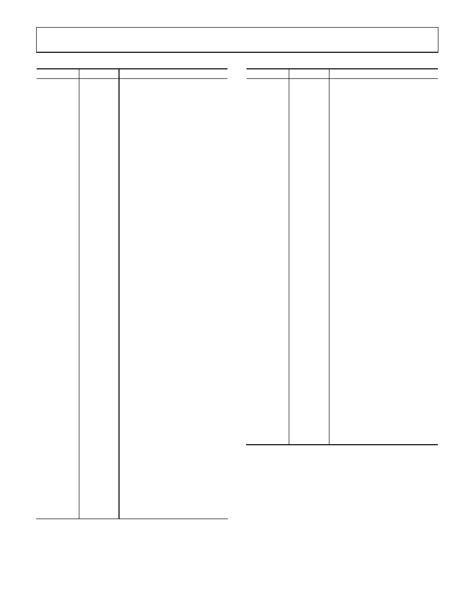
Table 7. Pin Function Descriptions—100-Lead TQFP/EP in LVDS Mode
Pin No.
Mnemonic
Description
1, 8 to 9,
16 to 18,
24 to 27,
34 to 35, 38,
41 to 42, 87,
89 to 95, 98
AVDD1
3.3 V (±5%) Analog Supply.
2 to 4
DNC
Do Not Connect. These pins
should float.
5
OUTPUT
MODE
CMOS Compatible Output Logic
Mode Control Pin. OUTPUT MODE
= 0 for CMOS mode, and OUTPUT
MODE = 1 (AVDD1) for LVDS
outputs.
6
DFS
Data Format Select Pin. CMOS
control pin that determines the
format of the output data. DFS =
high (AVDD1) for twos comple-
ment, DFS = low (ground) for
offset binary format.
7
LVDSBIAS
Set Pin for LVDS Output Current.
Place 3.7 k resistor terminated to
DRGND.
10
SENSE
Reference Mode Selection.
Connect to AGND for internal 1 V
reference, and connect to AVDD2
for external reference.
11
VREF
1.0 V Reference I/O—Function
Dependent on SENSE. Decouple
to ground with 0.1 F and 10 F
capacitors.
12, 15, 20,
23, 32, 86,
88, 96 to 97,
99, Exposed
Heat Sink
AGND
Analog Ground. The exposed
heat sink on the bottom of the
package must be connected to
AGND.
13
REFT
Differential Reference Output.
Decoupled to ground with 0.1 F
capacitor and to REFB (Pin 14) with
0.1 F and 10 F capacitors.
14
REFB
Differential Reference Output.
Decoupled to ground with a 0.1 F
capacitor and to REFT (Pin 13) with
0.1 F and 10 F capacitors.
19, 28 to 31,
39 to 40
AVDD2
5.0 V Analog Supply (±5%).
21
VIN+
Analog Input—True.
22
VIN
Analog Input—Complement.
33
C1
Internal Bypass Node. Connect a
0.1 F capacitor from this pin
to AGND.
36
CLK+
Clock Input—True.
37
CLK
Clock Input—Complement.
43
D0 (LSB)
D0 Complement Output Bit
(LVDS Levels).
Pin No.
Mnemonic
Description
44
D0+
D0 True Output Bit.
45
D1
D1 Complement Output Bit.
46
D1+
D1 True Output Bit.
47, 54, 62,
75, 83
DRVDD
3.3 V Digital Output Supply
(3.0 V to 3.6 V).
48, 53, 61,
67, 74, 82
DRGND
Digital Ground.
49
D2
D2 Complement Output Bit.
50
D2+
D2 True Output Bit.
51
D3
D3 Complement Output Bit.
52
D3+
D3 True Output Bit.
55
D4
D4 Complement Output Bit.
56
D4+
D4 True Output Bit.
57
D5
D5 Complement Output Bit.
58
D5+
D5 True Output Bit.
59
D6
D6 Complement Output Bit.
60
D6+
D6 True Output Bit.
63
DCO
Data Clock Output—Complement.
64
DCO+
Data Clock Output—True.
65
D7
D7 Complement Output Bit.
66
D7+
D7 True Output Bit.
68
D8
D8 Complement Output Bit.
69
D8+
D8 True Output Bit.
70
D9
D9 Complement Output Bit.
71
D9+
D9 True Output Bit.
72
D10
D10 Complement Output Bit.
73
D10+
D10 True Output Bit.
76
D11
D11 Complement Output Bit.
77
D11+
D11 True Output Bit.
78
D12
D12 Complement Output Bit.
79
D12+
D12 True Output Bit.
80
D13
D13 Complement Output.
81
D13+ (MSB)
D13 True Output Bit.
84
OR
Out-of-Range Complement
Output Bit.
85
OR+
Out-of-Range True Output Bit.
100
DCS MODE
Clock Duty Cycle Stabilizer (DCS)
Control Pin, CMOS-Compatible.
DCS = low (AGND) to enable DCS
(recommended). DCS = high
(AVDD1) to disable DCS.
相关PDF资料 |
PDF描述 |
|---|---|
| AD9445BSVZ-125 | IC ADC 14BIT 125MSPS 100-TQFP |
| AD9480BSUZ-250 | IC ADC 8BIT 250MSPS 3.3V 44TQFP |
| AD9481BSUZ-250 | IC ADC 8BIT 250MSPS 3.3V 44-TQFP |
| AD9484BCPZRL7-500 | IC ADC 8BIT 500MSPS 56LFCSP |
| AD9510BCPZ-REEL7 | IC CLOCK DIST 8OUT PLL 64LFCSP |
相关代理商/技术参数 |
参数描述 |
|---|---|
| AD9444-CMOS/PCB | 制造商:Analog Devices 功能描述:Evaluation Kit For 14-Bit, 80 MSPS, A/D Converter |
| AD9444-CMOSPCB | 制造商:AD 制造商全称:Analog Devices 功能描述:High Speed ADC USB FIFO Evaluation Kit |
| AD9444-LVDS/PCB | 制造商:Analog Devices 功能描述:14-BIT, 80 MSPS ADC PB FREE EVAL BD. - Trays |
| AD9444-LVDS/PCBZ | 制造商:Analog Devices 功能描述:LVDS Mode Evaluation Board 制造商:Analog Devices 功能描述:14-BIT, 80 MSPS ADC EVAL BD. - Bulk |
| AD9444-LVDSPCB | 制造商:AD 制造商全称:Analog Devices 功能描述:High Speed ADC USB FIFO Evaluation Kit |
发布紧急采购,3分钟左右您将得到回复。