参数资料
| 型号: | AD9577BCPZ-R7 |
| 厂商: | Analog Devices Inc |
| 文件页数: | 24/44页 |
| 文件大小: | 0K |
| 描述: | IC CLOCK GENERATOR 40LFCSP |
| 标准包装: | 750 |
| 系列: | PCI Express® (PCIe) |
| 类型: | 扇出缓冲器(分配),网络时钟发生器 |
| PLL: | 是 |
| 主要目的: | 以太网,PCI Express(PCIe),SONET/SDH |
| 输入: | 时钟,晶体 |
| 输出: | LVCMOS,LVDS,LVPECL |
| 电路数: | 1 |
| 比率 - 输入:输出: | 2:5 |
| 差分 - 输入:输出: | 无/是 |
| 频率 - 最大: | 637.5MHz |
| 电源电压: | 3 V ~ 3.6 V |
| 工作温度: | -40°C ~ 85°C |
| 安装类型: | 表面贴装 |
| 封装/外壳: | 40-WFQFN 裸露焊盘,CSP |
| 供应商设备封装: | 40-LFCSP-WQ(6x6) |
| 包装: | 带卷 (TR) |
| 其它名称: | AD9577BCPZ-R7TR |
第1页第2页第3页第4页第5页第6页第7页第8页第9页第10页第11页第12页第13页第14页第15页第16页第17页第18页第19页第20页第21页第22页第23页当前第24页第25页第26页第27页第28页第29页第30页第31页第32页第33页第34页第35页第36页第37页第38页第39页第40页第41页第42页第43页第44页
AD9577
Data Sheet
Rev. 0 | Page 30 of 44
OUTPUT CHANNEL DIVIDERS
Between each VCO and its associated chip outputs, there are
two divider stages: a VCO divider that has a divide ratio between
2 and 6 and an output divider that can be set to divide between
1 and 32. This cascade of dividers allows a minimum output
channel divide ratio of 2 and a maximum of 192. With VCO
frequencies ranging between 2.15 GHz and 2.55 GHz, the part
can be programmed to spot frequencies over a continuous
frequency range of from 11.2 MHz to 200 MHz, and it can be
programmed to spot frequencies over a continuous frequency
range of 200 MHz and 637.5 MHz, with only a few small gaps.
Table 19. Divider Ratio Setting Registers
Divider
I2C Registers
Parameter
Divide
Range
Channel 0 VCO divider
ADV0[7:5]
V0
2 to 6
Channel 1 VCO divider
ADV1[7:5]
V1
2 to 6
Channel 2 VCO divider
BDV0[7:5]
V2
2 to 6
Channel 3 VCO divider
BDV1[7:5]
V3
2 to 6
Channel 0 output divider
ADV0[4:0]
D0
Channel 1 output divider
ADV1[4:0]
D1
Channel 2 output divider
BDV0[4:0]
D2
Channel 3 output divider
BDV1[4:0]
D3
1 Set to 00000 for divide by 32.
Asserting the SyncCh01 or SyncCh23 bits (Register ADV2[0]
or Register BDV2[0]) allows each PLL output channel to use a
common VCO divider. This feature allows the OUT0/OUT1 and
OUT2/OUT3 output ports to have minimal skew when their
relative output channel divide ratio is an integer multiple.
Duty-cycle correction circuitry ensures that the output duty cycle
remains at 50%.
V0[2:0]
D0[4:0]
OUT0
OUTPUT
DIVIDER
VCO
DIVIDER
V1[2:0]
D1[4:0]
OUT1
OUTPUT
DIVIDER
VCO
DIVIDER
VCO
V2[2:0]
D2[4:0]
OUT2
OUTPUT
DIVIDER
VCO
DIVIDER
V3[2:0]
D3[4:0]
OUT3
OUTPUT
DIVIDER
VCO
DIVIDER
VCO
09
28
4-
0
39
Figure 35. Output Channel Divider Signal Path
OUTPUTS
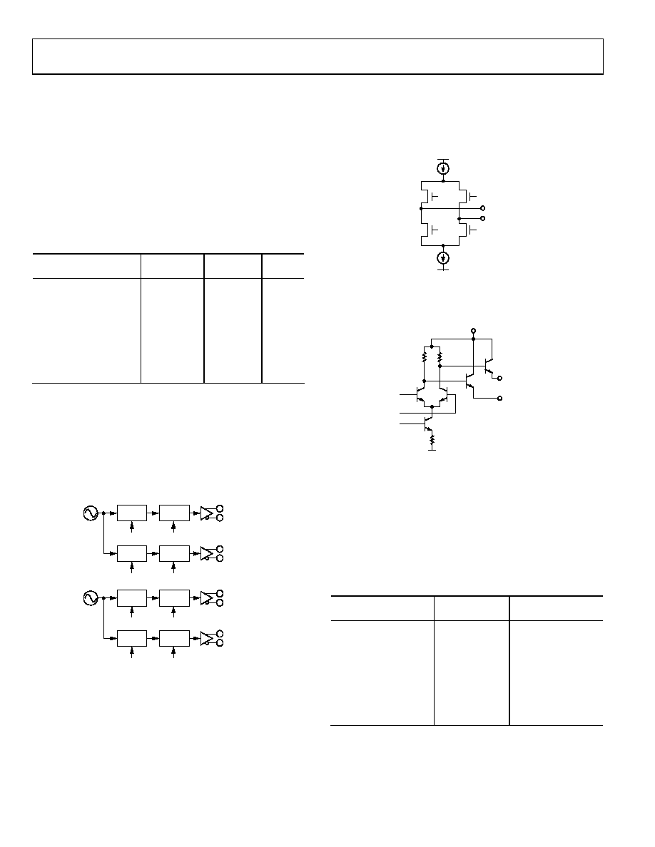
Each output port can be individually configured as either
differential LVPECL, differential LVDS, or two single-ended
LVCMOS clock outputs. The simplified equivalent circuit of the
LVDS outputs is shown in Figure 36.
3.5mA
OUTxP
OUTxN
09
284
-04
0
Figure 36. LVDS Outputs Simplified Equivalent Circuit
The simplified equivalent circuit of the LVPECL outputs is
shown in Figure 37.
3.3V
OUTxP
OUTxN
GND
092
84-
0
41
Figure 37. LVPECL Outputs Simplified Equivalent Circuit
Output channels (consisting of a VCO divider, output divider, and
an output buffer) can be individually powered down to save power.
Setting PDCH0, PDCH1, PDCH2, and PDCH3 (Register BP0[1:0]
and Register DR1[7:6]) powers down the appropriate channel.
Output buffer combinations of LVDS, LVPECL, and CMOS can be
Table 20. PLL1 Output Driver Format Control Bits,
Register DR1[2:0]
FORMAT1 (PLL1)
Register DR1[2:0]
OUT1P/OUT1N
OUT0P/OUT0N
000
LVPECL
001
LVDS
010
2 × CMOS
LVPECL
011
2 × CMOS
100
2 × CMOS
LVDS
101
LVPECL
LVDS
110
LVPECL
2 × CMOS
2 × CMOS
1 This indicates that the CMOS outputs are in phase; otherwise, they are in
antiphase.
相关PDF资料 |
PDF描述 |
|---|---|
| AD9600ABCPZ-150 | IC ADC 10BIT 150MSPS 64LFCSP |
| AD9608BCPZRL7-125 | IC ADC 10BIT 125MSPS 64LFCSP |
| AD9609BCPZRL7-80 | IC ADC 10BIT SRL/SPI 80M 32LFCSP |
| AD9613BCPZ-170 | IC ADC 12BIT SRL 170MSPS 64LFCSP |
| AD9627ABCPZ-125 | IC ADC 12BIT 1255MSPS 64LFCSP |
相关代理商/技术参数 |
参数描述 |
|---|---|
| AD9577BCPZ-RL | 功能描述:IC CLK GEN PLL DUAL 40LFCSP RoHS:是 类别:集成电路 (IC) >> 时钟/计时 - 专用 系列:PCI Express® (PCIe) 标准包装:28 系列:- 类型:时钟/频率发生器 PLL:是 主要目的:Intel CPU 服务器 输入:时钟 输出:LVCMOS 电路数:1 比率 - 输入:输出:3:22 差分 - 输入:输出:无/是 频率 - 最大:400MHz 电源电压:3.135 V ~ 3.465 V 工作温度:0°C ~ 85°C 安装类型:表面贴装 封装/外壳:64-TFSOP (0.240",6.10mm 宽) 供应商设备封装:64-TSSOP 包装:管件 |
| AD9577-EVALZ | 制造商:AD 制造商全称:Analog Devices 功能描述:Clock Generator with Dual PLLs |
| AD9578BCPZ | 功能描述:IC PLL CLOCK GEN 20MHZ 48LFCSP 制造商:analog devices inc. 系列:- 包装:托盘 零件状态:有效 类型:* PLL:带旁路 输入:LVCMOS,LVDS,LVPECL,晶体 输出:HCSL,LVCMOS,LVDS,LVPECL 电路数:1 比率 - 输入:输出:2:5 差分 - 输入:输出:是/是 频率 - 最大值:919MHz 分频器/倍频器:是/无 电压 - 电源:2.375 V ~ 3.63 V 工作温度:-25°C ~ 85°C 安装类型:表面贴装 封装/外壳:48-WFQFN 裸露焊盘,CSP 供应商器件封装:48-LFCSP-VQ(7x7) 标准包装:1 |
| AD9578BCPZ-REEL7 | 功能描述:IC PLL CLOCK GEN 20MHZ 48LFCSP 制造商:analog devices inc. 系列:- 包装:剪切带(CT) 零件状态:有效 类型:* PLL:带旁路 输入:LVCMOS,LVDS,LVPECL,晶体 输出:HCSL,LVCMOS,LVDS,LVPECL 电路数:1 比率 - 输入:输出:2:5 差分 - 输入:输出:是/是 频率 - 最大值:919MHz 分频器/倍频器:是/无 电压 - 电源:2.375 V ~ 3.63 V 工作温度:-25°C ~ 85°C 安装类型:表面贴装 封装/外壳:48-WFQFN 裸露焊盘,CSP 供应商器件封装:48-LFCSP-VQ(7x7) 标准包装:1 |
| AD95S08KAC | 制造商:未知厂家 制造商全称:未知厂家 功能描述:THYRISTOR MODULE|DOUBLER|HALF-CNTLD|POSITIVE|15V V(RRM)|95A I(T) |
发布紧急采购,3分钟左右您将得到回复。