参数资料
| 型号: | AD9577BCPZ-R7 |
| 厂商: | Analog Devices Inc |
| 文件页数: | 35/44页 |
| 文件大小: | 0K |
| 描述: | IC CLOCK GENERATOR 40LFCSP |
| 标准包装: | 750 |
| 系列: | PCI Express® (PCIe) |
| 类型: | 扇出缓冲器(分配),网络时钟发生器 |
| PLL: | 是 |
| 主要目的: | 以太网,PCI Express(PCIe),SONET/SDH |
| 输入: | 时钟,晶体 |
| 输出: | LVCMOS,LVDS,LVPECL |
| 电路数: | 1 |
| 比率 - 输入:输出: | 2:5 |
| 差分 - 输入:输出: | 无/是 |
| 频率 - 最大: | 637.5MHz |
| 电源电压: | 3 V ~ 3.6 V |
| 工作温度: | -40°C ~ 85°C |
| 安装类型: | 表面贴装 |
| 封装/外壳: | 40-WFQFN 裸露焊盘,CSP |
| 供应商设备封装: | 40-LFCSP-WQ(6x6) |
| 包装: | 带卷 (TR) |
| 其它名称: | AD9577BCPZ-R7TR |
第1页第2页第3页第4页第5页第6页第7页第8页第9页第10页第11页第12页第13页第14页第15页第16页第17页第18页第19页第20页第21页第22页第23页第24页第25页第26页第27页第28页第29页第30页第31页第32页第33页第34页当前第35页第36页第37页第38页第39页第40页第41页第42页第43页第44页
AD9577
Data Sheet
Rev. 0 | Page 40 of 44
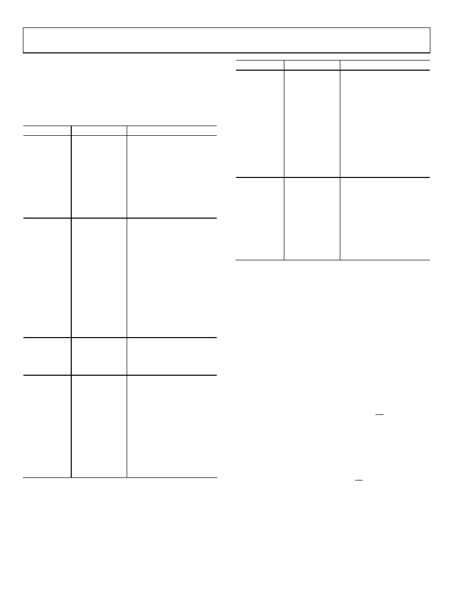
DEFAULT FREQUENCY MAP AND OUTPUT
FORMATS
The power-up operation (without I2C programming) of the
AD9577 is represented by a default frequency map and output
formats (see Table 31).
Table 31. Default Parameter Values, fPFD = 25 MHz
Parameter
Value
Notes
PLL1
fOUT0 = 156.25 MHz,
fOUT1 = 125 MHz
Na
80 + 20 = 100
V0
4
D0
4
V1
4
D1
5
FORMAT1
000
OUT0/OUT1 are LVPECL
SyncCh01
0
PLL2
fOUT2 = 100 MHz,
fOUT3 = 33.333 MHz
Nb
80 + 16 = 96
FRAC
0
MOD
0
PD_SDM
1
Bleed
0
V2
4
D2
6
V3
4
D3
18
FORMAT2
000
OUT2/OUT3 are LVPECL
SyncCh23
0
SSCG
FracStep
0
NumSteps
0
CkDiv
0
Control
EnI2C
0
NewAcq
0
PDCH0
0
PDCH1
0
PDCH2
0
PDCH3
0
PDRefOut
0
PDPLL1
0
PDPLL2
0
R
0
Parameter
Value
Notes
Margining
These parameters are
applied only when the
MARGIN pin = high
PLL1
fOUT0 = 156.25 MHz,
fOUT1 = 125 MHz
Na
80 + 20 = 100
V0
4
D0
4
V1
4
D1
5
fOUT0
156.25 MHz
fOUT1
125 MHz
PLL2
fOUT2 = 212.5 MHz,
fOUT3 = 106.25 MHz
Nb
80 + 22 = 102
FRAC
0
MOD
0
V2
2
D2
6
V3
4
D3
6
I2C INTERFACE OPERATION
driving multiple peripherals. Two inputs, serial data (SDA) and
serial clock (SCL), carry information between any devices
connected to the bus. Each slave device is recognized by a unique
address. The slave address consists of the 7 MSBs of an 8-bit
word. The 7-bit slave address of the AD9577 is 1000000. The LSB
of the word sets either a read or write operation (see Figure 44).
Logic 1 corresponds to a read operation, and Logic 0
corresponds to a write operation.
To control the device on the bus, do the following protocol.
First, the master initiates a data transfer by establishing a start
condition, defined by a high-to-low transition on SDA while
SCL remains high, which indicates that an address/data stream
follows. All peripherals respond to the start condition and shift
the next eight bits (the 7-bit address and the R/W bit). The bits
are transferred from MSB to LSB. The peripheral that recognizes
the transmitted address responds by pulling the data line low
during the ninth clock pulse, which is known as the acknowledge
bit. All other devices withdraw from the bus at this point and
maintain an idle condition. The idle condition is where the device
monitors the SDA and SCL lines waiting for the start condition
and correct transmitted address. The R/W bit determines the
direction of the data. Logic 0 on the LSB of the first byte means
that the master writes information to the peripheral, and Logic 1
on the LSB of the first byte means that the master reads
information from the peripheral.
相关PDF资料 |
PDF描述 |
|---|---|
| AD9600ABCPZ-150 | IC ADC 10BIT 150MSPS 64LFCSP |
| AD9608BCPZRL7-125 | IC ADC 10BIT 125MSPS 64LFCSP |
| AD9609BCPZRL7-80 | IC ADC 10BIT SRL/SPI 80M 32LFCSP |
| AD9613BCPZ-170 | IC ADC 12BIT SRL 170MSPS 64LFCSP |
| AD9627ABCPZ-125 | IC ADC 12BIT 1255MSPS 64LFCSP |
相关代理商/技术参数 |
参数描述 |
|---|---|
| AD9577BCPZ-RL | 功能描述:IC CLK GEN PLL DUAL 40LFCSP RoHS:是 类别:集成电路 (IC) >> 时钟/计时 - 专用 系列:PCI Express® (PCIe) 标准包装:28 系列:- 类型:时钟/频率发生器 PLL:是 主要目的:Intel CPU 服务器 输入:时钟 输出:LVCMOS 电路数:1 比率 - 输入:输出:3:22 差分 - 输入:输出:无/是 频率 - 最大:400MHz 电源电压:3.135 V ~ 3.465 V 工作温度:0°C ~ 85°C 安装类型:表面贴装 封装/外壳:64-TFSOP (0.240",6.10mm 宽) 供应商设备封装:64-TSSOP 包装:管件 |
| AD9577-EVALZ | 制造商:AD 制造商全称:Analog Devices 功能描述:Clock Generator with Dual PLLs |
| AD9578BCPZ | 功能描述:IC PLL CLOCK GEN 20MHZ 48LFCSP 制造商:analog devices inc. 系列:- 包装:托盘 零件状态:有效 类型:* PLL:带旁路 输入:LVCMOS,LVDS,LVPECL,晶体 输出:HCSL,LVCMOS,LVDS,LVPECL 电路数:1 比率 - 输入:输出:2:5 差分 - 输入:输出:是/是 频率 - 最大值:919MHz 分频器/倍频器:是/无 电压 - 电源:2.375 V ~ 3.63 V 工作温度:-25°C ~ 85°C 安装类型:表面贴装 封装/外壳:48-WFQFN 裸露焊盘,CSP 供应商器件封装:48-LFCSP-VQ(7x7) 标准包装:1 |
| AD9578BCPZ-REEL7 | 功能描述:IC PLL CLOCK GEN 20MHZ 48LFCSP 制造商:analog devices inc. 系列:- 包装:剪切带(CT) 零件状态:有效 类型:* PLL:带旁路 输入:LVCMOS,LVDS,LVPECL,晶体 输出:HCSL,LVCMOS,LVDS,LVPECL 电路数:1 比率 - 输入:输出:2:5 差分 - 输入:输出:是/是 频率 - 最大值:919MHz 分频器/倍频器:是/无 电压 - 电源:2.375 V ~ 3.63 V 工作温度:-25°C ~ 85°C 安装类型:表面贴装 封装/外壳:48-WFQFN 裸露焊盘,CSP 供应商器件封装:48-LFCSP-VQ(7x7) 标准包装:1 |
| AD95S08KAC | 制造商:未知厂家 制造商全称:未知厂家 功能描述:THYRISTOR MODULE|DOUBLER|HALF-CNTLD|POSITIVE|15V V(RRM)|95A I(T) |
发布紧急采购,3分钟左右您将得到回复。