- 您现在的位置:买卖IC网 > PDF目录10527 > AD9600ABCPZ-125 (Analog Devices Inc)IC ADC 10BIT 125MSPS 64LFCSP PDF资料下载
参数资料
| 型号: | AD9600ABCPZ-125 |
| 厂商: | Analog Devices Inc |
| 文件页数: | 29/72页 |
| 文件大小: | 0K |
| 描述: | IC ADC 10BIT 125MSPS 64LFCSP |
| 标准包装: | 1 |
| 位数: | 10 |
| 采样率(每秒): | 125M |
| 数据接口: | 串行,SPI? |
| 转换器数目: | 2 |
| 功率耗散(最大): | 800mW |
| 电压电源: | 模拟和数字 |
| 工作温度: | -40°C ~ 85°C |
| 安装类型: | 表面贴装 |
| 封装/外壳: | 64-VFQFN 裸露焊盘,CSP |
| 供应商设备封装: | 64-LFCSP-VQ(9x9) |
| 包装: | 托盘 |
| 输入数目和类型: | 4 个单端,单极;2 个差分,单极 |
第1页第2页第3页第4页第5页第6页第7页第8页第9页第10页第11页第12页第13页第14页第15页第16页第17页第18页第19页第20页第21页第22页第23页第24页第25页第26页第27页第28页当前第29页第30页第31页第32页第33页第34页第35页第36页第37页第38页第39页第40页第41页第42页第43页第44页第45页第46页第47页第48页第49页第50页第51页第52页第53页第54页第55页第56页第57页第58页第59页第60页第61页第62页第63页第64页第65页第66页第67页第68页第69页第70页第71页第72页
AD9600
Rev. B | Page 35 of 72
DC CORRECTION
Because the dc offset of the ADC may be significantly larger
than the signal being measured, a dc correction circuit is included
to null the dc offset before measuring the power. The dc correction
circuit can also be switched into the main signal path, but this
may not be appropriate if the ADC is digitizing a time-varying
signal with significant dc content, such as GSM.
DC Correction Bandwidth
The dc correction circuit is a high-pass filter with a programmable
bandwidth (ranging between 0.15 Hz and 1.2 kHz at 125 MSPS).
The bandwidth is controlled by writing the 4-bit dc correction
bandwidth register located at Register 0x10C, Bits [5:2].
The following equation can be used to compute the bandwidth
value for the dc correction circuit:
π
×
=
2
_
14
CLK
k
f
BW
Corr
DC
where:
k is the 4-bit value programmed in Register 0x10C, Bits [5:2]
(values between 0 and 13 are valid for k; programming 14 or
15 provides the same result as programming 13).
fCLK is the AD9600 ADC sample rate in hertz.
DC Correction Readback
The current dc correction value can be read back in Register 0x10D
and Register 0x10E for Channel A and Register 0x10F and
Register 0x110 for Channel B. The dc correction value is a 10-bit
value that can span the entire input range of the ADC.
DC Correction Freeze
Setting the dc correction freeze bit (Bit 6 of Register 0x10C) halts
the dc correction at its current state and continues to use the last
updated value as the dc correction value. Clearing this bit restarts
dc correction and adds the currently calculated value to the data.
DC Correction Enable Bits
Setting Bit 0 (the dc correction for SM enable bit) of Register 0x10C
enables the dc correction for use in the signal monitor calculations.
Setting Bit 1 (the dc correction for signal path enable bit) of
Register 0x10C enables the calculated dc correction value to
be added to the output data signal path.
SIGNAL MONITOR SPORT OUTPUT
The SPORT is a serial interface with three output pins:
SMI SCLK (SPORT clock), SMI SDFS (SPORT frame sync), and
SMI SDO (SPORT data). The SPORT is the master and drives
all three SPORT output pins on the chip.
SMI SCLK
The data and frame sync are driven on the positive edge of the
SMI SCLK. The SMI SCLK has three possible baud rates: 1/2, 1/4,
or 1/8 the ADC clock rate, based on the SPORT controls. In
addition, by using the SPORT SMI SCLK sleep bit, the SMI SCLK
can be gated to remain low when the signal monitor block is not
sending any data. Using this bit to disable the SMI SCLK when it is
not needed can reduce coupling errors in the return signal path.
Doing so, however, has the disadvantage of spreading the
frequency content of the clock; if desired, the SMI SCLK can be
left enabled to ease frequency planning.
SMI SDFS
The SMI SDFS is the serial data frame sync. It defines the start
of a frame. One SPORT frame includes data from both
datapaths. The data from Datapath A is sent just after the frame
sync, followed by data from Datapath B.
SMI SDO
The SMI SDO is the serial data output of the block. The data is sent
MSB first on the first positive edge after the SMI SDFS. Each data
output block includes one or more rms magnitude value, peak level
value, and threshold crossing value from each datapath in the stated
order. If enabled, the data is sent, rms first, followed by the peak
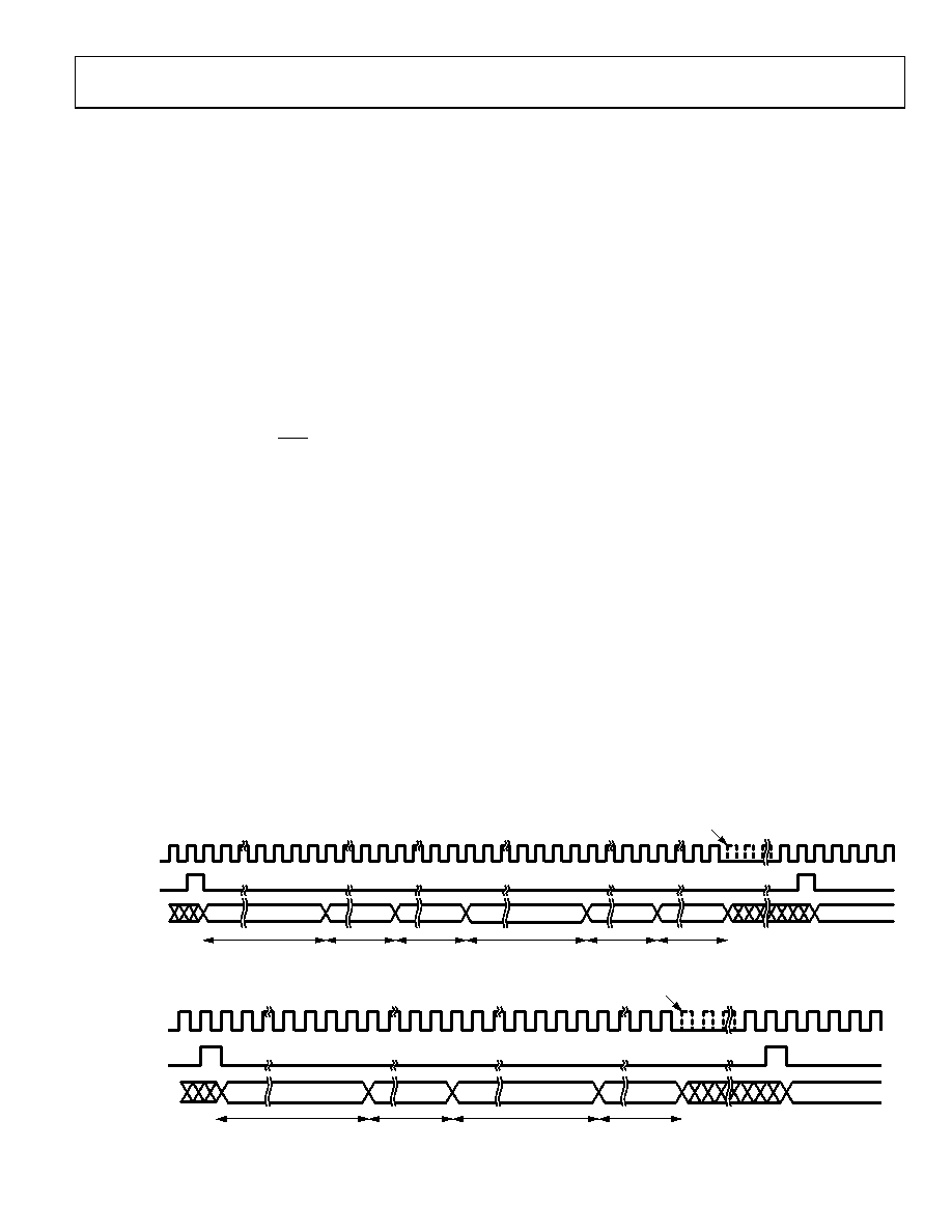
value and the threshold crossing value, as shown in Figure 70.
20 CYCLES
16 CYCLES
20 CYCLES
16 CYCLES
SMI SDFS
MSB
RMS/MS CH A
PK CH A
PK CH B
THR CH B
RMS/MS CH B
RMS/MS CH A
LSB
THR CH A
SMI SDO/OEB
SMI SCLK/PDWN
GATED, BASED ON CONTROL
06
909-
094
Figure 70. Signal Monitor SPORT Output Timing (RMS, Peak, and Threshold Enabled)
20 CYCLES
16 CYCLES
20 CYCLES
16 CYCLES
SMI SCLK/PDWN
SMI SDFS
SMI SDO/OEB
MSB
RMS/MS CH A
LSB
THR CH A
RMS/MS CH B LSB
THR CH B
GATED, BASED ON CONTROL
0
690
9-
0
95
Figure 71. Signal Monitor SPORT Output Timing (RMS and Threshold Enabled)
相关PDF资料 |
PDF描述 |
|---|---|
| ICL3237CAZ | IC 5DRVR/3RCVR RS232 3V 28-SSOP |
| AMIS42665TJAA1G | TRANSCEIVER CAN HS LP 8-SOIC |
| VE-J6W-MY-F2 | CONVERTER MOD DC/DC 5.5V 50W |
| ICL3243ECAZ | IC 3DRVR/5RCVR RS232 3V 28-SSOP |
| AD9054ABSTZ-135 | IC ADC 8BIT 135MSPS 44-LQFP |
相关代理商/技术参数 |
参数描述 |
|---|---|
| AD9600ABCPZ-150 | 功能描述:IC ADC 10BIT 150MSPS 64LFCSP RoHS:是 类别:集成电路 (IC) >> 数据采集 - 模数转换器 系列:- 标准包装:1 系列:- 位数:14 采样率(每秒):83k 数据接口:串行,并联 转换器数目:1 功率耗散(最大):95mW 电压电源:双 ± 工作温度:0°C ~ 70°C 安装类型:通孔 封装/外壳:28-DIP(0.600",15.24mm) 供应商设备封装:28-PDIP 包装:管件 输入数目和类型:1 个单端,双极 |
| AD9600BCPZ-105 | 制造商:Analog Devices 功能描述:ADC Dual Pipelined 105Msps 10-bit Parallel/LVDS 64-Pin LFCSP EP |
| AD9600BCPZ-125 | 制造商:Analog Devices 功能描述:ADC Dual Pipelined 125Msps 10-bit Parallel/LVDS 64-Pin LFCSP EP |
| AD9600BCPZ-150 | 制造商:Analog Devices 功能描述: |
| AD9601 | 制造商:AD 制造商全称:Analog Devices 功能描述:10-Bit, 200 MSPS/250 MSPS 1.8 V Analog-to-Digital Converter |
发布紧急采购,3分钟左右您将得到回复。