- 您现在的位置:买卖IC网 > PDF目录10527 > AD9600ABCPZ-125 (Analog Devices Inc)IC ADC 10BIT 125MSPS 64LFCSP PDF资料下载
参数资料
| 型号: | AD9600ABCPZ-125 |
| 厂商: | Analog Devices Inc |
| 文件页数: | 33/72页 |
| 文件大小: | 0K |
| 描述: | IC ADC 10BIT 125MSPS 64LFCSP |
| 标准包装: | 1 |
| 位数: | 10 |
| 采样率(每秒): | 125M |
| 数据接口: | 串行,SPI? |
| 转换器数目: | 2 |
| 功率耗散(最大): | 800mW |
| 电压电源: | 模拟和数字 |
| 工作温度: | -40°C ~ 85°C |
| 安装类型: | 表面贴装 |
| 封装/外壳: | 64-VFQFN 裸露焊盘,CSP |
| 供应商设备封装: | 64-LFCSP-VQ(9x9) |
| 包装: | 托盘 |
| 输入数目和类型: | 4 个单端,单极;2 个差分,单极 |
第1页第2页第3页第4页第5页第6页第7页第8页第9页第10页第11页第12页第13页第14页第15页第16页第17页第18页第19页第20页第21页第22页第23页第24页第25页第26页第27页第28页第29页第30页第31页第32页当前第33页第34页第35页第36页第37页第38页第39页第40页第41页第42页第43页第44页第45页第46页第47页第48页第49页第50页第51页第52页第53页第54页第55页第56页第57页第58页第59页第60页第61页第62页第63页第64页第65页第66页第67页第68页第69页第70页第71页第72页
AD9600
Rev. B | Page 39 of 72
CONFIGURATION WITHOUT THE SPI
In applications that do not interface to the SPI control registers,
the SDIO/DCS pin, the SCLK/DFS pin, the SMI SDO/OEB pin,
and the SMI SCLK/PDWN pin serve as standalone CMOS-
compatible control pins. When the device is powered up, it is
assumed that the user intends to use the pins as static control
lines for the duty cycle stabilizer, output data format, output
enable, and power-down feature control. In this mode, the CSB
chip select should be connected to AVDD, which disables the
serial port interface.
Table 20. Mode Selection
Pin
External
Voltage
Configuration
SDIO/DCS
AVDD (default)
Duty cycle stabilizer enabled
AGND
Duty cycle stabilizer disabled
SCLK/DFS
AVDD
Twos complement enabled
AGND (default)
Offset binary enabled
SMI SDO/OEB
AVDD
Outputs in high impedance
AGND (default)
Outputs enabled
SMI SCLK/PDWN
AVDD
Chip in power-down or
standby
AGND (default)
Normal operation
SPI ACCESSIBLE FEATURES
Brief descriptions of the general features available on many
Analog Devices, Inc., high speed ADCs, including the AD9600,
that are accessible via the SPI are included in Table 21. These
features are described in detail in the AN-877 Application Note,
Interfacing to High Speed ADCs via SPI. The AD9600 part-specific
features are described in the Memory Map Register Description
section.
Table 21. Features Accessible Using the SPI
Feature Name
Description
Modes
Allows the user to set either the power-down
mode or the standby mode
Clock
Allows the user to access the DCS via the SPI
Offset
Allows the user to digitally adjust the
converter offset
Test I/O
Allows the user to set the test modes to have
known data on the output bits
Output Mode
Allows the user to set up the outputs
Output Phase
Allows the user to set the output clock polarity
Output Delay
Allows the user to vary the DCO delay
VREF
Allows the user to set the reference voltage
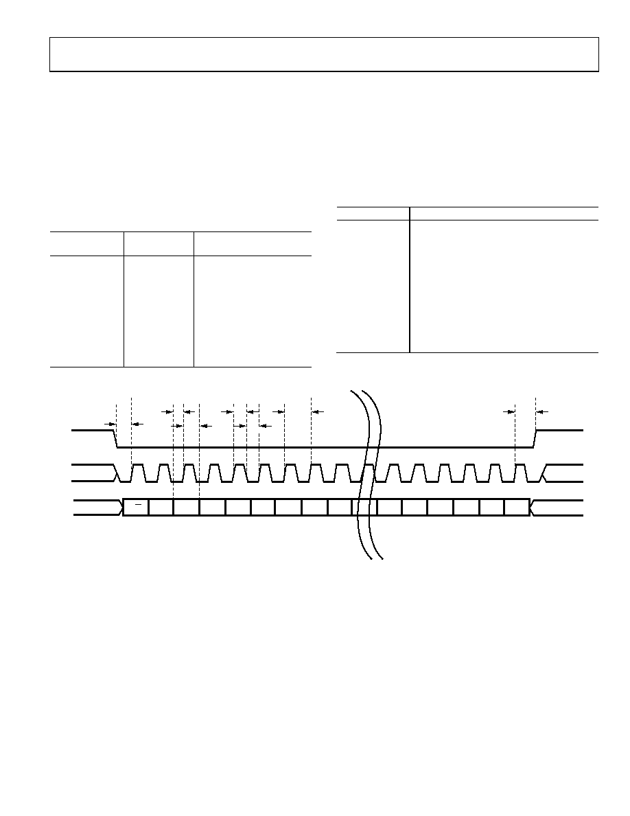
DON’T CARE
SDIO
SCLK
CSB
tS
tDH
tCLK
tDS
tH
R/W
W1
W0
A12
A11
A10
A9
A8
A7
D5
D4
D3
D2
D1
D0
tLOW
tHIGH
0
6909
-049
Figure 72. Serial Port Interface Timing Diagram
相关PDF资料 |
PDF描述 |
|---|---|
| ICL3237CAZ | IC 5DRVR/3RCVR RS232 3V 28-SSOP |
| AMIS42665TJAA1G | TRANSCEIVER CAN HS LP 8-SOIC |
| VE-J6W-MY-F2 | CONVERTER MOD DC/DC 5.5V 50W |
| ICL3243ECAZ | IC 3DRVR/5RCVR RS232 3V 28-SSOP |
| AD9054ABSTZ-135 | IC ADC 8BIT 135MSPS 44-LQFP |
相关代理商/技术参数 |
参数描述 |
|---|---|
| AD9600ABCPZ-150 | 功能描述:IC ADC 10BIT 150MSPS 64LFCSP RoHS:是 类别:集成电路 (IC) >> 数据采集 - 模数转换器 系列:- 标准包装:1 系列:- 位数:14 采样率(每秒):83k 数据接口:串行,并联 转换器数目:1 功率耗散(最大):95mW 电压电源:双 ± 工作温度:0°C ~ 70°C 安装类型:通孔 封装/外壳:28-DIP(0.600",15.24mm) 供应商设备封装:28-PDIP 包装:管件 输入数目和类型:1 个单端,双极 |
| AD9600BCPZ-105 | 制造商:Analog Devices 功能描述:ADC Dual Pipelined 105Msps 10-bit Parallel/LVDS 64-Pin LFCSP EP |
| AD9600BCPZ-125 | 制造商:Analog Devices 功能描述:ADC Dual Pipelined 125Msps 10-bit Parallel/LVDS 64-Pin LFCSP EP |
| AD9600BCPZ-150 | 制造商:Analog Devices 功能描述: |
| AD9601 | 制造商:AD 制造商全称:Analog Devices 功能描述:10-Bit, 200 MSPS/250 MSPS 1.8 V Analog-to-Digital Converter |
发布紧急采购,3分钟左右您将得到回复。