- 您现在的位置:买卖IC网 > PDF目录10534 > AD9608BCPZ-105 (Analog Devices Inc)IC ADC DUAL 10BIT 64-LFCSP PDF资料下载
参数资料
| 型号: | AD9608BCPZ-105 |
| 厂商: | Analog Devices Inc |
| 文件页数: | 21/40页 |
| 文件大小: | 0K |
| 描述: | IC ADC DUAL 10BIT 64-LFCSP |
| 标准包装: | 1 |
| 位数: | 10 |
| 采样率(每秒): | 105M |
| 数据接口: | LVDS,并联,串行,SPI |
| 转换器数目: | 2 |
| 电压电源: | 模拟和数字 |
| 工作温度: | -40°C ~ 85°C |
| 安装类型: | 表面贴装 |
| 封装/外壳: | 64-VFQFN 裸露焊盘,CSP |
| 供应商设备封装: | 64-LFCSP-VQ(9x9) |
| 包装: | 托盘 |
| 输入数目和类型: | 4 个单端,2 个差分 |
第1页第2页第3页第4页第5页第6页第7页第8页第9页第10页第11页第12页第13页第14页第15页第16页第17页第18页第19页第20页当前第21页第22页第23页第24页第25页第26页第27页第28页第29页第30页第31页第32页第33页第34页第35页第36页第37页第38页第39页第40页
AD9608
Rev. 0 | Page 28 of 40
Jitter Considerations
High speed, high resolution ADCs are sensitive to the quality
of the clock input. The degradation in SNR from the low fre-
quency SNR (SNRLF) at a given input frequency (fINPUT) due to
jitter (tJRMS) can be calculated by
SNRHF = 10 log[(2π × fINPUT × tJRMS)2 + 10
]
)
10
/
(
LF
SNR
In the previous equation, the rms aperture jitter represents the
clock input jitter specification. IF undersampling applications
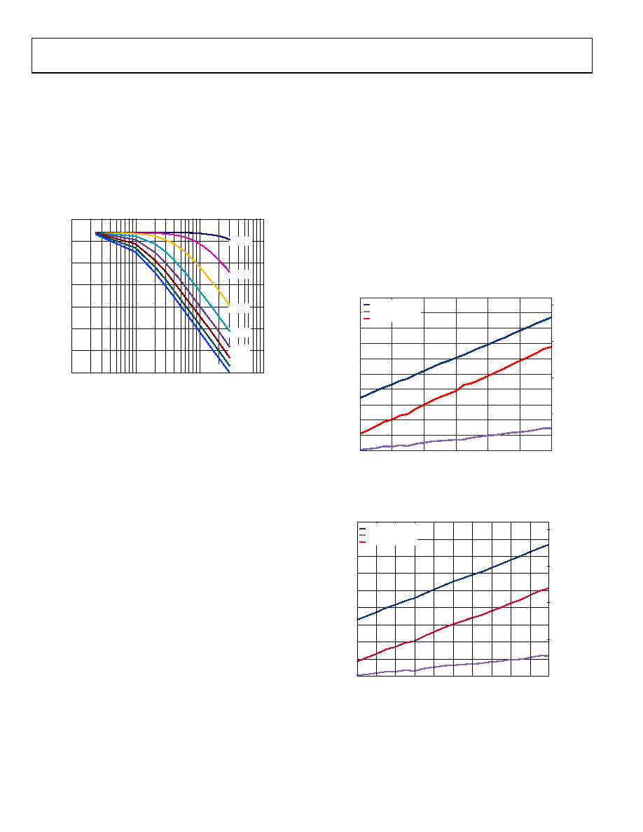
are particularly sensitive to jitter, as illustrated in Figure 59.
80
75
70
65
60
55
50
45
1
10
100
1k
FREQUENCY (MHz)
S
N
R
(dB
FS
)
0.5ps
0.2ps
0.05ps
1.0ps
1.5ps
2.0ps
2.5ps
3.0ps
099
77-
065
Figure 59. SNR vs. Input Frequency and Jitter
The clock input should be treated as an analog signal in cases
where aperture jitter may affect the dynamic range of the AD9608.
To avoid modulating the clock signal with digital noise, keep
power supplies for clock drivers separate from the ADC output
driver supplies. Low jitter, crystal-controlled oscillators make the
best clock sources. If the clock is generated from another type of
source (by gating, dividing, or another method), it should be
retimed by the original clock at the last step.
For more information, see the AN-501 Application Note and the
AN-756 Application Note, available on www.analog.com.
CHANNEL/CHIP SYNCHRONIZATION
The AD9608 has a SYNC input that offers the user flexible
synchronization options for synchronizing sample clocks
across multiple ADCs. The input clock divider can be enabled
to synchronize on a single occurrence of the SYNC signal or on
every occurrence. The SYNC input is internally synchronized
to the sample clock; however, to ensure that there is no timing
uncertainty between multiple parts, the SYNC input signal should
be externally synchronized to the input clock signal, meeting the
setup and hold times shown in Table 5. Drive the SYNC input
using a single-ended CMOS-type signal.
POWER DISSIPATION AND STANDBY MODE
As shown in Figure 60, the analog core power dissipated by
the AD9608 is proportional to its sample rate. The digital
power dissipation of the CMOS outputs are determined
primarily by the strength of the digital drivers and the load
on each output bit.
The maximum DRVDD current (IDRVDD) can be calculated as
IDRVDD = VDRVDD × CLOAD × fCLK × N
where N is the number of output bits (22, in the case of the
AD9608).
This maximum current occurs when every output bit switches
on every clock cycle, that is, a full-scale square wave at the Nyquist
frequency of fCLK/2. In practice, the DRVDD current is estab-
lished by the average number of output bits switching, which
is determined by the sample rate and the characteristics of the
analog input signal.
Reducing the capacitive load presented to the output drivers can
minimize digital power consumption. The data in Figure 60 was
taken in CMOS mode using the same operating conditions as those
used for the power supplies and power consumption parameters
in Table 1, with a 5 pF load on each output driver.
40
90
140
190
240
0
0.01
0.02
0.03
0.04
0.05
0.06
0.07
0.08
0.09
0.10
5
2545
6585
105
125
PO
W
ER
(m
W
)
S
UP
P
LY
CURRE
NT
(
mA)
ENCODE RATE (Msps)
IAVDD
IDRVDD
TOTAL POWER
0
9977-
03
0
Figure 60. AD9608-125 Power and Current vs. Clock Rate
(1.8 V CMOS Output Mode)
40
90
140
190
240
0
0.01
0.02
0.03
0.04
0.05
0.06
0.07
0.08
0.09
5
152535455565758595
105
P
OWE
R
(
m
W)
S
UP
P
LY
CU
RRE
N
T
(m
A)
ENCODE RATE (Msps)
IAVDD
IDRVDD
TOTAL POWER
0997
7-
0
23
Figure 61. AD9608-105 Power and Current vs. Clock Rate
(1.8 V CMOS Output Mode)
相关PDF资料 |
PDF描述 |
|---|---|
| VI-BTK-IV-F2 | CONVERTER MOD DC/DC 40V 150W |
| LTC1278-5CSW#PBF | IC A/DCONV SAMPLNG W/SHTDN24SOIC |
| LTC1278-5CSW | IC A/DCONV SAMPLNG W/SHTDN24SOIC |
| VI-BTJ-IV-F4 | CONVERTER MOD DC/DC 36V 150W |
| AD7777ARZ | IC ADC 10BIT 4CH HS 28SOIC |
相关代理商/技术参数 |
参数描述 |
|---|---|
| AD9608BCPZ-125 | 功能描述:IC ADC DUAL 10BIT 64-LFCSP RoHS:是 类别:集成电路 (IC) >> 数据采集 - 模数转换器 系列:- 其它有关文件:TSA1204 View All Specifications 标准包装:1 系列:- 位数:12 采样率(每秒):20M 数据接口:并联 转换器数目:2 功率耗散(最大):155mW 电压电源:模拟和数字 工作温度:-40°C ~ 85°C 安装类型:表面贴装 封装/外壳:48-TQFP 供应商设备封装:48-TQFP(7x7) 包装:Digi-Reel® 输入数目和类型:4 个单端,单极;2 个差分,单极 产品目录页面:1156 (CN2011-ZH PDF) 其它名称:497-5435-6 |
| AD9608BCPZRL7-105 | 功能描述:IC ADC 10BIT 105MSPS 64LFCSP RoHS:是 类别:集成电路 (IC) >> 数据采集 - 模数转换器 系列:- 标准包装:1,000 系列:- 位数:12 采样率(每秒):300k 数据接口:并联 转换器数目:1 功率耗散(最大):75mW 电压电源:单电源 工作温度:0°C ~ 70°C 安装类型:表面贴装 封装/外壳:24-SOIC(0.295",7.50mm 宽) 供应商设备封装:24-SOIC 包装:带卷 (TR) 输入数目和类型:1 个单端,单极;1 个单端,双极 |
| AD9608BCPZRL7-125 | 功能描述:IC ADC 10BIT 125MSPS 64LFCSP RoHS:是 类别:集成电路 (IC) >> 数据采集 - 模数转换器 系列:- 标准包装:1 系列:- 位数:14 采样率(每秒):83k 数据接口:串行,并联 转换器数目:1 功率耗散(最大):95mW 电压电源:双 ± 工作温度:0°C ~ 70°C 安装类型:通孔 封装/外壳:28-DIP(0.600",15.24mm) 供应商设备封装:28-PDIP 包装:管件 输入数目和类型:1 个单端,双极 |
| AD9609 | 制造商:AD 制造商全称:Analog Devices 功能描述:10-Bit, 20 MSPS/40 MSPS/65 MSPS/80 MSPS 1.8 V Analog-to-Digital Converter |
| AD9609-20EBZ | 功能描述:BOARD EVALUATION AD9609 20MSPS RoHS:是 类别:编程器,开发系统 >> 评估板 - 模数转换器 (ADC) 系列:- 产品培训模块:Obsolescence Mitigation Program 标准包装:1 系列:- ADC 的数量:1 位数:12 采样率(每秒):94.4k 数据接口:USB 输入范围:±VREF/2 在以下条件下的电源(标准):- 工作温度:-40°C ~ 85°C 已用 IC / 零件:MAX11645 已供物品:板,软件 |
发布紧急采购,3分钟左右您将得到回复。