- 您现在的位置:买卖IC网 > PDF目录8652 > AD9741BCPZRL (Analog Devices Inc)IC DAC DUAL 8BIT 250MSPS 72LFCSP PDF资料下载
参数资料
| 型号: | AD9741BCPZRL |
| 厂商: | Analog Devices Inc |
| 文件页数: | 10/28页 |
| 文件大小: | 0K |
| 描述: | IC DAC DUAL 8BIT 250MSPS 72LFCSP |
| 产品培训模块: | Data Converter Fundamentals DAC Architectures |
| 标准包装: | 2,000 |
| 位数: | 8 |
| 数据接口: | 并联 |
| 转换器数目: | 2 |
| 电压电源: | 模拟和数字 |
| 功率耗散(最大): | 345mW |
| 工作温度: | -40°C ~ 85°C |
| 安装类型: | 表面贴装 |
| 封装/外壳: | 72-VFQFN 裸露焊盘,CSP |
| 供应商设备封装: | 72-LFCSP |
| 包装: | 带卷 (TR) |
| 输出数目和类型: | 4 电流,单极 |
| 采样率(每秒): | 250M |
第1页第2页第3页第4页第5页第6页第7页第8页第9页当前第10页第11页第12页第13页第14页第15页第16页第17页第18页第19页第20页第21页第22页第23页第24页第25页第26页第27页第28页
AD9741/AD9743/AD9745/AD9746/AD9747
Data Sheet
Rev. A | Page 18 of 28
THEORY OF OPERATION
many features to make them very attractive for wired and
wireless communications systems. The dual DAC architecture
facilitates easy interfacing to common quadrature modulators
when designing single sideband transmitters. In addition, the
speed and performance of the devices allow wider bandwidths
and more carriers to be synthesized than in previously available
products.
All features and options are software programmable through
the SPI port.
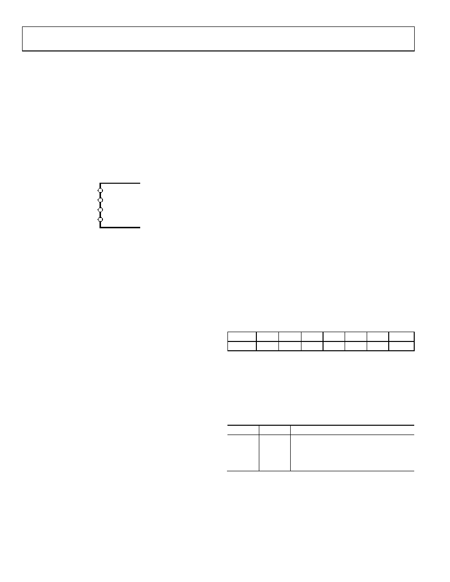
SERIAL PERIPHERAL INTERFACE
AD9747
SPI
PORT
SDO
SDIO
SCLK
CSB
06569-
013
Figure 22. SPI Port
The SPI port is a flexible, synchronous serial communications
port allowing easy interfacing to many industry-standard
microcontrollers and microprocessors. The port is compatible
with most synchronous transfer formats including both the
Motorola SPI and Intel
SSR protocols.
The interface allows read and write access to all registers that
Single or multiple byte transfers are supported as well as MSB-
first or LSB-first transfer formats. Serial data input/output can
be accomplished through a single bidirectional pin (SDIO) or
through two unidirectional pins (SDIO/SDO).
The serial port configuration is controlled by Register 0x00,
Bits<7:6>. It is important to note that any change made to the
serial port configuration occurs immediately upon writing to
the last bit of this byte. Therefore, it is possible with a multibyte
transfer to write to this register and change the configuration in
the middle of a communication cycle. Care must be taken to
compensate for the new configuration within the remaining
bytes of the current communication cycle.
Use of a single-byte transfer when changing the serial port
configuration is recommended to prevent unexpected device
behavior.
GENERAL OPERATION OF THE SERIAL INTERFACE
There are two phases to any communication cycle with the
Phase 2. Phase 1 is the instruction cycle, which writes an
instruction byte into the device. This byte provides the serial
port controller with information regarding Phase 2 of the
communication cycle: the data transfer cycle.
The Phase 1 instruction byte defines whether the upcoming
data transfer is read or write, the number of bytes in the data
transfer, and a reference register address for the first byte of the
data transfer. A logic high on the CSB pin followed by a logic
low resets the SPI port to its initial state and defines the start
of the instruction cycle. From this point, the next eight rising
SCLK edges define the eight bits of the instruction byte for the
current communication cycle.
The remaining SCLK edges are for Phase 2 of the communication
cycle, which is the data transfer between the serial port control-
ler and the system controller. Phase 2 can be a transfer of 1, 2, 3,
or 4 data bytes as determined by the instruction byte. Using
multibyte transfers is usually preferred although single-byte
data transfers are useful to reduce CPU overhead or when only
a single register access is required.
All serial port data is transferred to and from the device in syn-
chronization with the SCLK pin. Input data is always latched
on the rising edge of SCLK whereas output data is always valid
after the falling edge of SCLK. Register contents change imme-
diately upon writing to the last bit of each transfer byte.
When synchronization is lost, the device has the ability to
asynchronously terminate an I/O operation whenever the CSB
pin is taken to logic high. Any unwritten register content data is
lost if the I/O operation is aborted. Taking CSB low then resets the
serial port controller and restarts the communication cycle.
INSTRUCTION BYTE
The instruction byte contains the information shown in the
following bit map.
MSB
LSB
B7
B6
B5
B4
B3
B2
B1
B0
R/W
N1
N0
A4
A3
A2
A1
A0
Bit 7, R/W, determines whether a read or a write data transfer
occurs after the instruction byte write. Logic high indicates a
read operation. Logic 0 indicates a write operation.
Bits<6:5>, N1 and N0, determine the number of bytes to be
transferred during the data transfer cycle. The bits decode as
shown in Table 13.
Table 13. Byte Transfer Count
N1
N0
Description
0
Transfer one byte
0
1
Transfer two bytes
1
0
Transfer three bytes
1
Transfer four bytes
Bits<4:0>, A4, A3, A2, A1, and A0, determine which register is
accessed during the data transfer of the communications cycle.
For multibyte transfers, this address is a starting or ending
address depending on the current data transfer mode. For MSB-
first format, the specified address is an ending address or the
most significant address in the current cycle. Remaining
register addresses for multiple byte data transfers are generated
相关PDF资料 |
PDF描述 |
|---|---|
| IDT74FCT807BTQI | IC CLK BUFFER 1:10 100MHZ 20QSOP |
| IDT74FCT807BTQ8 | IC CLK BUFFER 1:10 100MHZ 20QSOP |
| AD5556CRU-REEL7 | IC DAC 14BIT PARAL IN 28TSSOP TR |
| IDT74FCT807BTQ | IC CLK BUFFER 1:10 100MHZ 20QSOP |
| VI-J63-MZ-B1 | CONVERTER MOD DC/DC 24V 25W |
相关代理商/技术参数 |
参数描述 |
|---|---|
| AD9741-DPG2-EBZ | 功能描述:IC DAC DUAL 8BIT 200MSPS 72LFCSP RoHS:是 类别:编程器,开发系统 >> 评估板 - 数模转换器 (DAC) 系列:- 产品培训模块:Lead (SnPb) Finish for COTS Obsolescence Mitigation Program 标准包装:1 系列:- DAC 的数量:4 位数:12 采样率(每秒):- 数据接口:串行,SPI? 设置时间:3µs DAC 型:电流/电压 工作温度:-40°C ~ 85°C 已供物品:板 已用 IC / 零件:MAX5581 |
| AD9741-EBZ | 制造商:Analog Devices 功能描述:Evaluation Board For AD9741 制造商:Analog Devices 功能描述:DUAL 8BIT, 200 MSPS D-A CONVERTER - Bulk |
| AD9742 | 制造商:AD 制造商全称:Analog Devices 功能描述:Analog Devices: Data Converters: DAC 12-Bit, 10 ns to 100 ns Converters Selection Table |
| AD9742ACP | 制造商:Analog Devices 功能描述:DAC 1-CH Segment 12-bit 32-Pin LFCSP EP 制造商:Rochester Electronics LLC 功能描述:12-BIT 165 MSPS TXDAC D/A CONVERTER - Bulk 制造商:Analog Devices 功能描述:IC 12-BIT DAC |
| AD9742ACP-PCB | 制造商:Analog Devices 功能描述:EVAL BD FOR AD9742 12BIT, 165MSPS TXDAC D/A CNVRTR - Bulk |
发布紧急采购,3分钟左右您将得到回复。