- 您现在的位置:买卖IC网 > PDF目录8652 > AD9741BCPZRL (Analog Devices Inc)IC DAC DUAL 8BIT 250MSPS 72LFCSP PDF资料下载
参数资料
| 型号: | AD9741BCPZRL |
| 厂商: | Analog Devices Inc |
| 文件页数: | 16/28页 |
| 文件大小: | 0K |
| 描述: | IC DAC DUAL 8BIT 250MSPS 72LFCSP |
| 产品培训模块: | Data Converter Fundamentals DAC Architectures |
| 标准包装: | 2,000 |
| 位数: | 8 |
| 数据接口: | 并联 |
| 转换器数目: | 2 |
| 电压电源: | 模拟和数字 |
| 功率耗散(最大): | 345mW |
| 工作温度: | -40°C ~ 85°C |
| 安装类型: | 表面贴装 |
| 封装/外壳: | 72-VFQFN 裸露焊盘,CSP |
| 供应商设备封装: | 72-LFCSP |
| 包装: | 带卷 (TR) |
| 输出数目和类型: | 4 电流,单极 |
| 采样率(每秒): | 250M |
第1页第2页第3页第4页第5页第6页第7页第8页第9页第10页第11页第12页第13页第14页第15页当前第16页第17页第18页第19页第20页第21页第22页第23页第24页第25页第26页第27页第28页
Data Sheet
AD9741/AD9743/AD9745/AD9746/AD9747
Rev. A | Page 23 of 28
In pin mode, all register bits are reset to their default values
with the exception of those that are controlled by the SPI pins.
Note also that the RESET pin should be allowed to float and
must be pulled low. Connect an external 10 kΩ resistor to
DVSS. This avoids unexpected behavior in noisy environments.
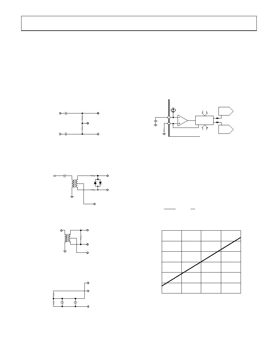
DRIVING THE DAC CLOCK INPUT
The DAC clock input requires a low jitter drive signal. It is a
PMOS differential pair powered from the CVDD18 supply.
Each pin can safely swing up to 800 mV p-p at a common-
mode voltage of about 400 mV. Though these levels are not
directly LVDS-compatible, CLKP and CLKN can be driven by
an ac-coupled, dc-offset LVDS signal, as shown in Figure 29.
LVDS_P_IN
CLKP
50
0.1F
LVDS_N_IN
CLKN
VCM = 400mV
06569-
021
Figure 29. LVDS DAC Clock Drive Circuit
Using a CMOS or TTL clock is also acceptable for lower sample
rates. It can be routed through an LVDS translator and then
ac-coupled as described previously, or alternatively, it can be
transformer-coupled and clamped, as shown in Figure 30.
50
TTL OR CMOS
CLK INPUT
CLKP
CLKN
VCM = 400mV
BAV99ZXCT
HIGH SPEED
DUAL DIODE
0.1F
06569-
022
Figure 30. TTL or CMOS DAC Clock Drive Circuit
If a sine wave signal is available, it can be transformer-coupled
directly to the DAC clock inputs, as shown in Figure 31.
50
SINE WAVE
INPUT
CLKP
CLKN
VCM = 400mV
06569-
034
Figure 31. Sine Wave DAC Clock Drive Circuit
The 400 mV common-mode bias voltage can be derived from
the CVDD18 supply through a simple divider network, as
shown in Figure 32.
0.1F
1nF
VCM = 400mV
CVDD18
CVSS
1k
287
06569-
023
Figure 32. DAC Clock VCM Circuit
It is important to use CVDD18 and CVSS for any clock bias
circuit as noise that is coupled onto the clock from another
power supply is multiplied by the DAC input signal and
degrades performance.
FULL-SCALE CURRENT GENERATION
The full-scale currents on DAC1 and DAC2 are functions of
the current drawn through an external resistor connected to
the FSADJ pin (Pin 54). The required value for this resistor is
10 kΩ. An internal amplifier sets the current through the
resistor to force a voltage equal to the band gap voltage of 1.2 V.
This develops a reference current in the resistor of 120 μA.
CURRENT
SCALING
1.2V BANDGAP
DAC1 GAIN
DAC2 GAIN
AD9747
DAC1
DAC2
DAC FULL SCALE
REFERENCE CURRENT
REFIO
FSADJ
0.1F
10k
06569-
024
Figure 33. Reference Circuitry
REFIO (Pin 55) should be bypassed to ground with a 0.1 μF
capacitor. The band gap voltage is present on this pin and can
be buffered for use in external circuitry. The typical output
impedance is near 5 kΩ. If desired, an external reference can
be connected to REFIO to overdrive the internal reference.
Internal current mirrors provide a means for adjusting the
DAC full-scale currents. The gain for DAC1 and DAC2 can be
adjusted independently by writing to the DAC1FSC<9:0> and
DAC2FSC<9:0> register bits. The default value of 0x01F9 for
the DAC gain registers gives an IFS of 20 mA, where IFS equals
×
+
×
=
FSC
DAC
IFS
n
16
3
72
10,000
V
1.2
The full-scale output current range is 8.6 mA to 31.7 mA for
register values 0x000 to 0x3FF.
06569-
025
35
30
25
20
15
10
5
I FS
(
mA)
0
256
512
768
1024
DAC GAIN CODE
Figure 34. IFS vs. DAC Gain Code
相关PDF资料 |
PDF描述 |
|---|---|
| IDT74FCT807BTQI | IC CLK BUFFER 1:10 100MHZ 20QSOP |
| IDT74FCT807BTQ8 | IC CLK BUFFER 1:10 100MHZ 20QSOP |
| AD5556CRU-REEL7 | IC DAC 14BIT PARAL IN 28TSSOP TR |
| IDT74FCT807BTQ | IC CLK BUFFER 1:10 100MHZ 20QSOP |
| VI-J63-MZ-B1 | CONVERTER MOD DC/DC 24V 25W |
相关代理商/技术参数 |
参数描述 |
|---|---|
| AD9741-DPG2-EBZ | 功能描述:IC DAC DUAL 8BIT 200MSPS 72LFCSP RoHS:是 类别:编程器,开发系统 >> 评估板 - 数模转换器 (DAC) 系列:- 产品培训模块:Lead (SnPb) Finish for COTS Obsolescence Mitigation Program 标准包装:1 系列:- DAC 的数量:4 位数:12 采样率(每秒):- 数据接口:串行,SPI? 设置时间:3µs DAC 型:电流/电压 工作温度:-40°C ~ 85°C 已供物品:板 已用 IC / 零件:MAX5581 |
| AD9741-EBZ | 制造商:Analog Devices 功能描述:Evaluation Board For AD9741 制造商:Analog Devices 功能描述:DUAL 8BIT, 200 MSPS D-A CONVERTER - Bulk |
| AD9742 | 制造商:AD 制造商全称:Analog Devices 功能描述:Analog Devices: Data Converters: DAC 12-Bit, 10 ns to 100 ns Converters Selection Table |
| AD9742ACP | 制造商:Analog Devices 功能描述:DAC 1-CH Segment 12-bit 32-Pin LFCSP EP 制造商:Rochester Electronics LLC 功能描述:12-BIT 165 MSPS TXDAC D/A CONVERTER - Bulk 制造商:Analog Devices 功能描述:IC 12-BIT DAC |
| AD9742ACP-PCB | 制造商:Analog Devices 功能描述:EVAL BD FOR AD9742 12BIT, 165MSPS TXDAC D/A CNVRTR - Bulk |
发布紧急采购,3分钟左右您将得到回复。