- 您现在的位置:买卖IC网 > PDF目录8652 > AD9741BCPZRL (Analog Devices Inc)IC DAC DUAL 8BIT 250MSPS 72LFCSP PDF资料下载
参数资料
| 型号: | AD9741BCPZRL |
| 厂商: | Analog Devices Inc |
| 文件页数: | 18/28页 |
| 文件大小: | 0K |
| 描述: | IC DAC DUAL 8BIT 250MSPS 72LFCSP |
| 产品培训模块: | Data Converter Fundamentals DAC Architectures |
| 标准包装: | 2,000 |
| 位数: | 8 |
| 数据接口: | 并联 |
| 转换器数目: | 2 |
| 电压电源: | 模拟和数字 |
| 功率耗散(最大): | 345mW |
| 工作温度: | -40°C ~ 85°C |
| 安装类型: | 表面贴装 |
| 封装/外壳: | 72-VFQFN 裸露焊盘,CSP |
| 供应商设备封装: | 72-LFCSP |
| 包装: | 带卷 (TR) |
| 输出数目和类型: | 4 电流,单极 |
| 采样率(每秒): | 250M |
第1页第2页第3页第4页第5页第6页第7页第8页第9页第10页第11页第12页第13页第14页第15页第16页第17页当前第18页第19页第20页第21页第22页第23页第24页第25页第26页第27页第28页
AD9741/AD9743/AD9745/AD9746/AD9747
Data Sheet
Rev. A | Page 25 of 28
0
–10
–20
–30
–40
T
(f)
(d
B
)
0.5
1.5
2
FS
NORMAL
RZ
MIX
06569-
027
Figure 36. Transfer Function for Each Analog Operating Mode
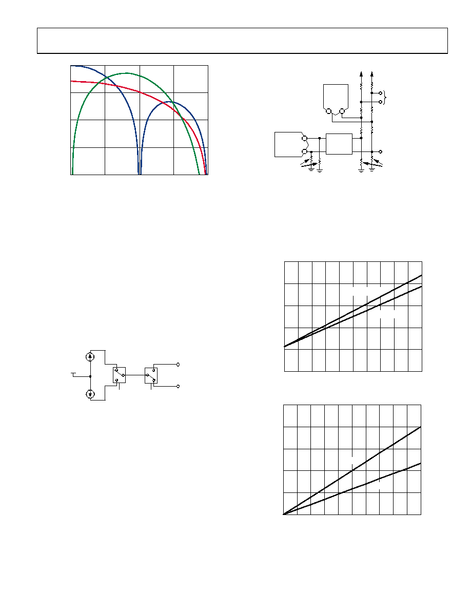
AUXILIARY DACS
in Figure 37. The auxiliary DACs are current output devices
with two output pins, AUXP and AUXN. The active pin can
be programmed to either source or sink current. When either
sinking or sourcing, the full-scale current magnitude is 2 mA.
The available compliance range at the auxiliary DAC outputs
depends on whether the output is configured to a sink or source
current. When sourcing current, the compliance voltage is 0 V
to 1.6 V, but when sinking current, the output compliance
voltage reduces to 0.8 V to 1.6 V. Either output can be used, but
only one output of the auxiliary DAC (P or N) is active at any
time. The inactive pin is always in a high impedance state
(>100 kΩ).
06569-
035
VBIAS
AUXP
AUXN
SINK
OR
SOURCE
POSITIVE
OR
NEGATIVE
0mA
TO
2mA
0mA
TO
2mA
Figure 37. Auxiliary DAC Functional Diagram
In a single side band transmitter application, the combination of
the input referred dc offset voltage of the quadrature modulator
and the DAC output offset voltage can result in local oscillator
(LO) feedthrough at the modulator output, which degrades
system performance. The auxiliary DACs can be used to remove
the dc offset and the resulting LO feedthrough. The circuit
configuration for using the auxiliary DACs for performing
dc offset correction depends on the details of the DAC and
modulator interface. An example of a dc-coupled configuration
with low-pass filtering is outlined in the Power Dissipation
section.
AD9747
AUX
DAC1 OR
DAC2
AD9747
DAC1 OR
DAC2
25 TO 50
QUAD MOD
I OR Q INPUTS
QUADRATURE
MODULATOR V+
25 TO 50
06569-
029
OPTIONAL
PASSIVE
FILTERING
Figure 38. DAC DC Coupled to Quadrature Modulator with Passive DC Shift
POWER DISSIPATION
Figure 39 shows the power dissipation and current draw of the
devices have a quiescent power dissipation of about 190 mW.
Most of this comes from the AVDD33 supply. Total power
dissipation increases about 50% as the clock rate is increased
to the maximum clock rate of 250 MHz.
350
310
270
230
190
150
P
TO
TA
L
(
mW
)
0
50
100
150
200
250
fDAC (MHz)
06569-
030
25
75
125
175
225
fOUT = DC
fOUT = NYQUIST
Figure 39. AD9747 Power Dissipation vs. fDAC
15
12
9
6
3
0
I DV
DD3
3
(
mA)
0
50
100
150
200
250
fDAC (MHz)
06569-
031
25
75
125
175
225
AD9747
AD9741
Figure 40. DVDD33 Current vs. fDAC
相关PDF资料 |
PDF描述 |
|---|---|
| IDT74FCT807BTQI | IC CLK BUFFER 1:10 100MHZ 20QSOP |
| IDT74FCT807BTQ8 | IC CLK BUFFER 1:10 100MHZ 20QSOP |
| AD5556CRU-REEL7 | IC DAC 14BIT PARAL IN 28TSSOP TR |
| IDT74FCT807BTQ | IC CLK BUFFER 1:10 100MHZ 20QSOP |
| VI-J63-MZ-B1 | CONVERTER MOD DC/DC 24V 25W |
相关代理商/技术参数 |
参数描述 |
|---|---|
| AD9741-DPG2-EBZ | 功能描述:IC DAC DUAL 8BIT 200MSPS 72LFCSP RoHS:是 类别:编程器,开发系统 >> 评估板 - 数模转换器 (DAC) 系列:- 产品培训模块:Lead (SnPb) Finish for COTS Obsolescence Mitigation Program 标准包装:1 系列:- DAC 的数量:4 位数:12 采样率(每秒):- 数据接口:串行,SPI? 设置时间:3µs DAC 型:电流/电压 工作温度:-40°C ~ 85°C 已供物品:板 已用 IC / 零件:MAX5581 |
| AD9741-EBZ | 制造商:Analog Devices 功能描述:Evaluation Board For AD9741 制造商:Analog Devices 功能描述:DUAL 8BIT, 200 MSPS D-A CONVERTER - Bulk |
| AD9742 | 制造商:AD 制造商全称:Analog Devices 功能描述:Analog Devices: Data Converters: DAC 12-Bit, 10 ns to 100 ns Converters Selection Table |
| AD9742ACP | 制造商:Analog Devices 功能描述:DAC 1-CH Segment 12-bit 32-Pin LFCSP EP 制造商:Rochester Electronics LLC 功能描述:12-BIT 165 MSPS TXDAC D/A CONVERTER - Bulk 制造商:Analog Devices 功能描述:IC 12-BIT DAC |
| AD9742ACP-PCB | 制造商:Analog Devices 功能描述:EVAL BD FOR AD9742 12BIT, 165MSPS TXDAC D/A CNVRTR - Bulk |
发布紧急采购,3分钟左右您将得到回复。