- 您现在的位置:买卖IC网 > PDF目录8652 > AD9741BCPZRL (Analog Devices Inc)IC DAC DUAL 8BIT 250MSPS 72LFCSP PDF资料下载
参数资料
| 型号: | AD9741BCPZRL |
| 厂商: | Analog Devices Inc |
| 文件页数: | 15/28页 |
| 文件大小: | 0K |
| 描述: | IC DAC DUAL 8BIT 250MSPS 72LFCSP |
| 产品培训模块: | Data Converter Fundamentals DAC Architectures |
| 标准包装: | 2,000 |
| 位数: | 8 |
| 数据接口: | 并联 |
| 转换器数目: | 2 |
| 电压电源: | 模拟和数字 |
| 功率耗散(最大): | 345mW |
| 工作温度: | -40°C ~ 85°C |
| 安装类型: | 表面贴装 |
| 封装/外壳: | 72-VFQFN 裸露焊盘,CSP |
| 供应商设备封装: | 72-LFCSP |
| 包装: | 带卷 (TR) |
| 输出数目和类型: | 4 电流,单极 |
| 采样率(每秒): | 250M |
第1页第2页第3页第4页第5页第6页第7页第8页第9页第10页第11页第12页第13页第14页当前第15页第16页第17页第18页第19页第20页第21页第22页第23页第24页第25页第26页第27页第28页
AD9741/AD9743/AD9745/AD9746/AD9747
Data Sheet
Rev. A | Page 22 of 28
DIGITAL INPUTS AND OUTPUTS
in two data input modes: dual-port mode and single-port mode.
For the default dual-port mode (ONEPORT = 0), each DAC
receives data from a dedicated input port. In single-port mode
(ONEPORT = 1), however, both DACs receive data from Port 1.
In single-port mode, DAC1 and DAC2 data is interleaved and
the IQSEL input is used to steer data to the correct DAC.
In single-port mode, when the IQSEL input is high, Port 1
data is delivered to DAC1 and when IQSEL is low, Port 1 data
is delivered to DAC2. The IQSEL input should always coincide
and be time-aligned with the other data bus signals. In single-
port mode, minimum setup and hold times apply to the IQSEL
input as well as to the input data signals. In dual-port mode, the
IQSEL input is ignored.
In dual-port mode, the data must be delivered at the sample rate
(up to 250 MSPS). In single-port mode, data must be delivered
at twice the sample rate. Because the data inputs function only
up to 250 MSPS, it is only practical to operate the DAC clock at
up to 125 MHz in single-port mode.
In both dual-port and single-port modes, a data clock output
(DCO) signal is available as a fixed time base with which to
stimulate data from an FPGA. This output signal always
operates at the sample rate. It may be inverted by asserting
the INVDCO bit.
INPUT DATA TIMING
With most DACs, signal-to-noise ratio (SNR) is a function of
the relationship between the position of the clock edges and the
point in time at which the input data changes. The AD9741/
and thus exhibit greater SNR sensitivity when the data tran-
sition is close to this edge.
The specified minimum setup and hold times define a window
of time, within each data period, where the data is sampled
correctly. Generally, users should position data to arrive
relative to the DAC clock and well beyond the minimum
setup and minimum hold times. This becomes increasingly
more important at increasingly higher sample rates.
DUAL-PORT MODE TIMING
The timing diagram for the dual-port mode is shown in
CLKP/CLKN
DCO
P1D<15:0>
P2D<15:0>
tDCO
tDBH
tDBS
06569-
018
I1
I2
I3
I4
Q1
Q2
Q3
Q4
Figure 27. Data Interface Timing, Dual-Port Mode
In Figure 27, data samples for DAC1 are labeled Ix and data
samples for DAC2 are labeled Qx. Note that the differential
DAC clock input is shown in a logical sense (CLKP/CLKN).
The data clock output is labeled DCO.
Setup and hold times are referenced to the positive transition of
the DAC clock. Data should arrive at the input pins such that
the minimum setup and hold times are met. Note that the data
clock output has a fixed time delay from the DAC clock and
may be a more convenient signal to use to confirm timing.
SINGLE-PORT MODE TIMING
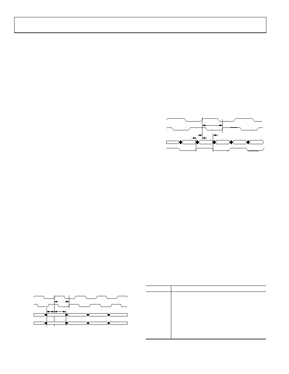
The single-port mode timing diagram is shown in Figure 28.
06569-
019
CLKP/CLKN
DCO
P1D<15:0>
IQSEL
tDBS
tDBH
tDCO
I1
Q1
I2
Q2
Figure 28. Data Interface Timing, Single-Port Mode
In single-port mode, data for both DACs is received on the
Port 1 input bus. Ix and Qx data samples are interleaved and
arrive twice as fast as in dual-port mode. Accompanying the
data is the IQSEL input signal, which steers incoming data to its
respective DAC. When IQSEL is high, data is steered to DAC1
and when IQSEL is low, data is steered to DAC2. IQSEL should
coincide as well as be time-aligned with incoming data.
SPI PORT, RESET, AND PIN MODE
AD9747 are powered up, an active high pulse applied to the
RESET pin should follow. This insures the default state of all
control register bits. In addition, once the RESET pin goes low,
the SPI port can be activated, so CSB should be held high.
which allows some functional options to be pin, selected with-
out the use of the SPI port. Pin mode is enabled anytime the
RESET pin is held high. In pin mode, the four SPI port pins
take on secondary functions, as shown in Table 16.
Table 16. SPI Pin Functions (Pin Mode)
Pin Name
Pin Mode Description
SCLK
ONEPORT (Register 0x02, Bit 6), bit value (1/0)
equals pin state (high/low)
SDIO
DATTYPE (Register 0x02, Bit 7), bit value (1/0)
equals pin state (high/low)
CSB
Enable Mix Mode, if CSB is high, Register 0x0A
is set to 0x05 putting both DAC1 and DAC2 into
mix mode
SDO
Enable full power-down, if SDO is high, Register
0x03 is set to 0xFF
相关PDF资料 |
PDF描述 |
|---|---|
| IDT74FCT807BTQI | IC CLK BUFFER 1:10 100MHZ 20QSOP |
| IDT74FCT807BTQ8 | IC CLK BUFFER 1:10 100MHZ 20QSOP |
| AD5556CRU-REEL7 | IC DAC 14BIT PARAL IN 28TSSOP TR |
| IDT74FCT807BTQ | IC CLK BUFFER 1:10 100MHZ 20QSOP |
| VI-J63-MZ-B1 | CONVERTER MOD DC/DC 24V 25W |
相关代理商/技术参数 |
参数描述 |
|---|---|
| AD9741-DPG2-EBZ | 功能描述:IC DAC DUAL 8BIT 200MSPS 72LFCSP RoHS:是 类别:编程器,开发系统 >> 评估板 - 数模转换器 (DAC) 系列:- 产品培训模块:Lead (SnPb) Finish for COTS Obsolescence Mitigation Program 标准包装:1 系列:- DAC 的数量:4 位数:12 采样率(每秒):- 数据接口:串行,SPI? 设置时间:3µs DAC 型:电流/电压 工作温度:-40°C ~ 85°C 已供物品:板 已用 IC / 零件:MAX5581 |
| AD9741-EBZ | 制造商:Analog Devices 功能描述:Evaluation Board For AD9741 制造商:Analog Devices 功能描述:DUAL 8BIT, 200 MSPS D-A CONVERTER - Bulk |
| AD9742 | 制造商:AD 制造商全称:Analog Devices 功能描述:Analog Devices: Data Converters: DAC 12-Bit, 10 ns to 100 ns Converters Selection Table |
| AD9742ACP | 制造商:Analog Devices 功能描述:DAC 1-CH Segment 12-bit 32-Pin LFCSP EP 制造商:Rochester Electronics LLC 功能描述:12-BIT 165 MSPS TXDAC D/A CONVERTER - Bulk 制造商:Analog Devices 功能描述:IC 12-BIT DAC |
| AD9742ACP-PCB | 制造商:Analog Devices 功能描述:EVAL BD FOR AD9742 12BIT, 165MSPS TXDAC D/A CNVRTR - Bulk |
发布紧急采购,3分钟左右您将得到回复。