- 您现在的位置:买卖IC网 > PDF目录17065 > AD9752-EBZ (Analog Devices Inc)BOARD EVAL FOR AD9752 PDF资料下载
参数资料
| 型号: | AD9752-EBZ |
| 厂商: | Analog Devices Inc |
| 文件页数: | 4/23页 |
| 文件大小: | 0K |
| 描述: | BOARD EVAL FOR AD9752 |
| 标准包装: | 1 |
| 系列: | TxDAC® |
| DAC 的数量: | 1 |
| 位数: | 12 |
| 采样率(每秒): | 125M |
| 数据接口: | 并联 |
| 设置时间: | 35ns |
| DAC 型: | 电流 |
| 工作温度: | -40°C ~ 85°C |
| 已供物品: | 板 |
| 已用 IC / 零件: | AD9752 |
REV. 0
AD9752
–12–
In summary, the AD9752 achieves the optimum distortion and
noise performance under the following conditions:
(1) Differential Operation.
(2) Positive voltage swing at IOUTA and IOUTB limited to
+0.5 V.
(3) IOUTFS set to 20 mA.
(4) Analog Supply (AVDD) set at 5.0 V.
(5) Digital Supply (DVDD) set at 3.0 V to 3.3 V with appro-
priate logic levels.
Note that the ac performance of the AD9752 is characterized
under the above mentioned operating conditions.
DIGITAL INPUTS
The AD9752’s digital input consists of 12 data input pins and a
clock input pin. The 12-bit parallel data inputs follow standard
positive binary coding where DB11 is the most significant bit
(MSB) and DB0 is the least significant bit (LSB). IOUTA
produces a full-scale output current when all data bits are at
Logic 1. IOUTB produces a complementary output with the
full-scale current split between the two outputs as a function of
the input code.
The digital interface is implemented using an edge-triggered
master slave latch. The DAC output is updated following the
rising edge of the clock as shown in Figure 1 and is designed to
support a clock rate as high as 125 MSPS. The clock can be
operated at any duty cycle that meets the specified latch pulse-
width. The setup and hold times can also be varied within the
clock cycle as long as the specified minimum times are met;
although the location of these transition edges may affect digital
feedthrough and distortion performance. Best performance is
typically achieved when the input data transitions on the falling edge
of a 50% duty cycle clock.
The digital inputs are CMOS compatible with logic thresholds,
VTHRESHOLD set to approximately half the digital positive supply
(DVDD) or
VTHRESHOLD = DVDD/2 (± 20%)
The internal digital circuitry of the AD9752 is capable of operating
over a digital supply range of 2.7 V to 5.5 V. As a result, the
digital inputs can also accommodate TTL levels when DVDD is
set to accommodate the maximum high level voltage of the TTL
drivers VOH(MAX). A DVDD of 3 V to 3.3 V will typically ensure
proper compatibility with most TTL logic families. Figure 23
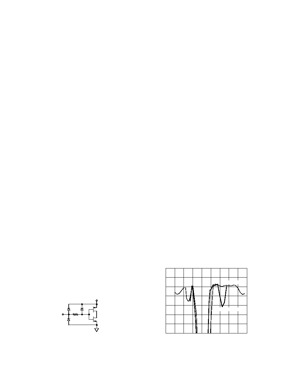
shows the equivalent digital input circuit for the data and clock
inputs. The sleep mode input is similar with the exception that
it contains an active pull-down circuit, thus ensuring that the
AD9752 remains enabled if this input is left disconnected.
DVDD
DIGITAL
INPUT
Figure 23. Equivalent Digital Input
Since the AD9752 is capable of being updated up to 125 MSPS,
the quality of the clock and data input signals are important in
achieving the optimum performance. The drivers of the digital
data interface circuitry should be specified to meet the mini-
mum setup and hold times of the AD9752 as well as its re-
quired min/max input logic level thresholds. Typically, the
selection of the slowest logic family that satisfies the above con-
ditions will result in the lowest data feedthrough and noise.
Digital signal paths should be kept short and run lengths
matched to avoid propagation delay mismatch. The insertion of
a low value resistor network (i.e., 20
to 100 ) between the
AD9752 digital inputs and driver outputs may be helpful in reduc-
ing any overshooting and ringing at the digital inputs that con-
tribute to data feedthrough. For longer run lengths and high data
update rates, strip line techniques with proper termination resis-
tors should be considered to maintain “clean” digital inputs. Also,
operating the AD9752 with reduced logic swings and a corre-
sponding digital supply (DVDD) will also reduce data feedthrough.
The external clock driver circuitry should provide the AD9752
with a low jitter clock input meeting the min/max logic levels
while providing fast edges. Fast clock edges will help minimize
any jitter that will manifest itself as phase noise on a recon-
structed waveform. Thus, the clock input should be driven by
the fastest logic family suitable for the application.
Note, the clock input could also be driven via a sine wave, which is
centered around the digital threshold (i.e., DVDD/2), and meets
the min/max logic threshold. This will typically result in a slight
degradation in the phase noise, which becomes more noticeable
at higher sampling rates and output frequencies. Also, at higher
sampling rates, the 20% tolerance of the digital logic threshold
should be considered since it will affect the effective clock duty
cycle and subsequently cut into the required data setup and
hold times.
INPUT CLOCK/DATA TIMING RELATIONSHIP
SNR in a DAC is dependent on the relationship between the
position of the clock edges and the point in time at which the
input data changes. The AD9752 is positive edge triggered, and
so exhibits SNR sensitivity when the data transition is close to
this edge. In general, the goal when applying the AD9752 is to
make the data transitions shortly after the positive clock edge.
This becomes more important as the sample rate increases. Figure
24 shows the relationship of SNR to clock placement with dif-
ferent sample rates and different frequencies out. Note that at
the lower sample rates, much more tolerance is allowed in clock
placement, while at higher rates, much more care must be taken.
TIME OF DATA CHANGE RELATIVE TO
RISING CLOCK EDGE – ns
68
40
–8
10
–6
–4
–2
0
2
4
6
8
64
60
56
52
48
SNR
–
dB
44
FS = 65MSPS
FS = 125MSPS
Figure 24. SNR vs. Clock Placement @ fOUT = 10 MHz
相关PDF资料 |
PDF描述 |
|---|---|
| AD9754-EBZ | BOARD EVAL FOR AD9754 |
| 380LX680M400J202 | CAP ALUM 68UF 400V 20% SNAP |
| SDR0302-2R2ML | INDUCTOR POWER 2.2UH 1.65A 0302 |
| AD9750-EB | BOARD EVAL FOR AD9750 |
| UPS2E471MRD | CAP ALUM 470UF 250V 20% RADIAL |
相关代理商/技术参数 |
参数描述 |
|---|---|
| AD9753 | 制造商:AD 制造商全称:Analog Devices 功能描述:Analog Devices: Data Converters: DAC 12-Bit, 10 ns to 100 ns Converters Selection Table |
| AD9753AST | 制造商:Analog Devices 功能描述:DAC 1-CH Segment 12-bit 48-Pin LQFP 制造商:Rochester Electronics LLC 功能描述:12-BIT, 300 MSPS TXDAC+ D/A CONVERTER - Tape and Reel 制造商:Analog Devices 功能描述:IC 12-BIT DAC |
| AD9753ASTRL | 制造商:Analog Devices 功能描述:DAC 1-CH Segment 12-bit 48-Pin LQFP T/R 制造商:Rochester Electronics LLC 功能描述:12-BIT, 300 MSPS TXDAC+ D/A CONVERTER - Tape and Reel |
| AD9753ASTZ | 功能描述:IC DAC 12BIT 300MSPS 48-LQFP RoHS:是 类别:集成电路 (IC) >> 数据采集 - 数模转换器 系列:TxDAC+® 标准包装:1 系列:- 设置时间:4.5µs 位数:12 数据接口:串行,SPI? 转换器数目:1 电压电源:单电源 功率耗散(最大):- 工作温度:-40°C ~ 125°C 安装类型:表面贴装 封装/外壳:8-SOIC(0.154",3.90mm 宽) 供应商设备封装:8-SOICN 包装:剪切带 (CT) 输出数目和类型:1 电压,单极;1 电压,双极 采样率(每秒):* 其它名称:MCP4921T-E/SNCTMCP4921T-E/SNRCTMCP4921T-E/SNRCT-ND |
| AD9753ASTZRL | 功能描述:IC DAC 12BIT 300MSPS 48LQFP RoHS:是 类别:集成电路 (IC) >> 数据采集 - 数模转换器 系列:TxDAC+® 产品培训模块:Lead (SnPb) Finish for COTS Obsolescence Mitigation Program 标准包装:1,000 系列:- 设置时间:1µs 位数:8 数据接口:串行 转换器数目:8 电压电源:双 ± 功率耗散(最大):941mW 工作温度:0°C ~ 70°C 安装类型:表面贴装 封装/外壳:24-SOIC(0.295",7.50mm 宽) 供应商设备封装:24-SOIC W 包装:带卷 (TR) 输出数目和类型:8 电压,单极 采样率(每秒):* |
发布紧急采购,3分钟左右您将得到回复。