- 您现在的位置:买卖IC网 > PDF目录17065 > AD9752-EBZ (Analog Devices Inc)BOARD EVAL FOR AD9752 PDF资料下载
参数资料
| 型号: | AD9752-EBZ |
| 厂商: | Analog Devices Inc |
| 文件页数: | 5/23页 |
| 文件大小: | 0K |
| 描述: | BOARD EVAL FOR AD9752 |
| 标准包装: | 1 |
| 系列: | TxDAC® |
| DAC 的数量: | 1 |
| 位数: | 12 |
| 采样率(每秒): | 125M |
| 数据接口: | 并联 |
| 设置时间: | 35ns |
| DAC 型: | 电流 |
| 工作温度: | -40°C ~ 85°C |
| 已供物品: | 板 |
| 已用 IC / 零件: | AD9752 |
REV. 0
AD9752
–13–
SLEEP MODE OPERATION
The AD9752 has a power-down function which turns off the
output current and reduces the supply current to less than
8.5 mA over the specified supply range of 2.7 V to 5.5 V and
temperature range. This mode can be activated by applying a
logic level “1” to the SLEEP pin. This digital input also con-
tains an active pull-down circuit that ensures the AD9752 re-
mains enabled if this input is left disconnected. The AD9752
takes less than 50 ns to power down and approximately 5
s to
power back up.
POWER DISSIPATION
The power dissipation, PD, of the AD9752 is dependent on
several factors which include: (1) AVDD and DVDD, the
power supply voltages; (2) IOUTFS, the full-scale current output;
(3) fCLOCK, the update rate; (4) and the reconstructed digital
input waveform. The power dissipation is directly proportional
to the analog supply current, IAVDD, and the digital supply cur-
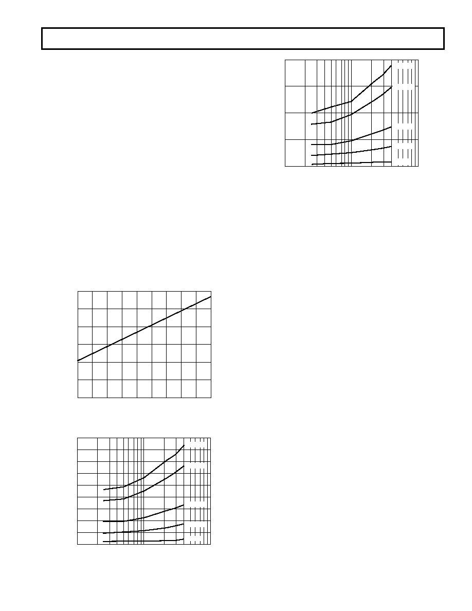
rent, IDVDD. IAVDD is directly proportional to IOUTFS as shown in
Figure 25 and is insensitive to fCLOCK.
Conversely, IDVDD is dependent on both the digital input wave-
form, fCLOCK, and digital supply DVDD. Figures 26 and 27
show IDVDD as a function of full-scale sine wave output ratios
(fOUT/fCLOCK) for various update rates with DVDD = 5 V and
DVDD = 3 V, respectively. Note, how IDVDD is reduced by more
than a factor of 2 when DVDD is reduced from 5 V to 3 V.
IOUTFS – mA
35
5
220
4
6
8
10
12
141618
30
25
20
15
10
I AVDD
–
mA
Figure 25. IAVDD vs. IOUTFS
RATIO (fCLOCK/fOUT)
18
16
0
0.01
1
0.1
I DVDD
–
mA
8
6
4
2
12
10
14
125MSPS
100MSPS
50MSPS
25MSPS
5MSPS
Figure 26. IDVDD vs. Ratio @ DVDD = 5 V
RATIO (fCLOCK/fOUT)
8
0
0.01
1
0.1
I DVDD
–
mA
6
4
2
125MSPS
100MSPS
50MSPS
25MSPS
5MSPS
Figure 27. IDVDD vs. Ratio @ DVDD = 3 V
APPLYING THE AD9752
OUTPUT CONFIGURATIONS
The following sections illustrate some typical output configura-
tions for the AD9752. Unless otherwise noted, it is assumed
that IOUTFS is set to a nominal 20 mA. For applications requir-
ing the optimum dynamic performance, a differential output
configuration is suggested. A differential output configuration
may consist of either an RF transformer or a differential op amp
configuration. The transformer configuration provides the opti-
mum high frequency performance and is recommended for any
application allowing for ac coupling. The differential op amp
configuration is suitable for applications requiring dc coupling, a
bipolar output, signal gain and/or level shifting.
A single-ended output is suitable for applications requiring a
unipolar voltage output. A positive unipolar output voltage will
result if IOUTA and/or IOUTB is connected to an appropri-
ately sized load resistor, RLOAD, referred to ACOM. This con-
figuration may be more suitable for a single-supply system
requiring a dc coupled, ground referred output voltage. Alterna-
tively, an amplifier could be configured as an I-V converter thus
converting IOUTA or IOUTB into a negative unipolar voltage.
This configuration provides the best dc linearity since IOUTA
or IOUTB is maintained at a virtual ground. Note, IOUTA
provides slightly better performance than IOUTB.
DIFFERENTIAL COUPLING USING A TRANSFORMER
An RF transformer can be used to perform a differential-to-
single-ended signal conversion as shown in Figure 28. A
differentially coupled transformer output provides the optimum
distortion performance for output signals whose spectral content
lies within the transformer’s passband. An RF transformer such
as the Mini-Circuits T1-1T provides excellent rejection of
common-mode distortion (i.e., even-order harmonics) and noise
over a wide frequency range. It also provides electrical isolation
and the ability to deliver twice the power to the load. Trans-
formers with different impedance ratios may also be used for
impedance matching purposes. Note that the transformer
provides ac coupling only.
相关PDF资料 |
PDF描述 |
|---|---|
| AD9754-EBZ | BOARD EVAL FOR AD9754 |
| 380LX680M400J202 | CAP ALUM 68UF 400V 20% SNAP |
| SDR0302-2R2ML | INDUCTOR POWER 2.2UH 1.65A 0302 |
| AD9750-EB | BOARD EVAL FOR AD9750 |
| UPS2E471MRD | CAP ALUM 470UF 250V 20% RADIAL |
相关代理商/技术参数 |
参数描述 |
|---|---|
| AD9753 | 制造商:AD 制造商全称:Analog Devices 功能描述:Analog Devices: Data Converters: DAC 12-Bit, 10 ns to 100 ns Converters Selection Table |
| AD9753AST | 制造商:Analog Devices 功能描述:DAC 1-CH Segment 12-bit 48-Pin LQFP 制造商:Rochester Electronics LLC 功能描述:12-BIT, 300 MSPS TXDAC+ D/A CONVERTER - Tape and Reel 制造商:Analog Devices 功能描述:IC 12-BIT DAC |
| AD9753ASTRL | 制造商:Analog Devices 功能描述:DAC 1-CH Segment 12-bit 48-Pin LQFP T/R 制造商:Rochester Electronics LLC 功能描述:12-BIT, 300 MSPS TXDAC+ D/A CONVERTER - Tape and Reel |
| AD9753ASTZ | 功能描述:IC DAC 12BIT 300MSPS 48-LQFP RoHS:是 类别:集成电路 (IC) >> 数据采集 - 数模转换器 系列:TxDAC+® 标准包装:1 系列:- 设置时间:4.5µs 位数:12 数据接口:串行,SPI? 转换器数目:1 电压电源:单电源 功率耗散(最大):- 工作温度:-40°C ~ 125°C 安装类型:表面贴装 封装/外壳:8-SOIC(0.154",3.90mm 宽) 供应商设备封装:8-SOICN 包装:剪切带 (CT) 输出数目和类型:1 电压,单极;1 电压,双极 采样率(每秒):* 其它名称:MCP4921T-E/SNCTMCP4921T-E/SNRCTMCP4921T-E/SNRCT-ND |
| AD9753ASTZRL | 功能描述:IC DAC 12BIT 300MSPS 48LQFP RoHS:是 类别:集成电路 (IC) >> 数据采集 - 数模转换器 系列:TxDAC+® 产品培训模块:Lead (SnPb) Finish for COTS Obsolescence Mitigation Program 标准包装:1,000 系列:- 设置时间:1µs 位数:8 数据接口:串行 转换器数目:8 电压电源:双 ± 功率耗散(最大):941mW 工作温度:0°C ~ 70°C 安装类型:表面贴装 封装/外壳:24-SOIC(0.295",7.50mm 宽) 供应商设备封装:24-SOIC W 包装:带卷 (TR) 输出数目和类型:8 电压,单极 采样率(每秒):* |
发布紧急采购,3分钟左右您将得到回复。