- 您现在的位置:买卖IC网 > PDF目录17064 > AD9778A-DPG2-EBZ (Analog Devices Inc)BOARD EVALUATION FOR AD9778A PDF资料下载
参数资料
| 型号: | AD9778A-DPG2-EBZ |
| 厂商: | Analog Devices Inc |
| 文件页数: | 20/56页 |
| 文件大小: | 0K |
| 描述: | BOARD EVALUATION FOR AD9778A |
| 标准包装: | 1 |
| 系列: | * |
| DAC 的数量: | 2 |
| 位数: | 14 |
| 采样率(每秒): | 1G |
| 数据接口: | 并联 |
| DAC 型: | 电流 |
| 工作温度: | -40°C ~ 85°C |
| 已供物品: | * |
| 已用 IC / 零件: | AD9778A |
第1页第2页第3页第4页第5页第6页第7页第8页第9页第10页第11页第12页第13页第14页第15页第16页第17页第18页第19页当前第20页第21页第22页第23页第24页第25页第26页第27页第28页第29页第30页第31页第32页第33页第34页第35页第36页第37页第38页第39页第40页第41页第42页第43页第44页第45页第46页第47页第48页第49页第50页第51页第52页第53页第54页第55页第56页
AD9776A/AD9778A/AD9779A
Rev. B | Page 27 of 56
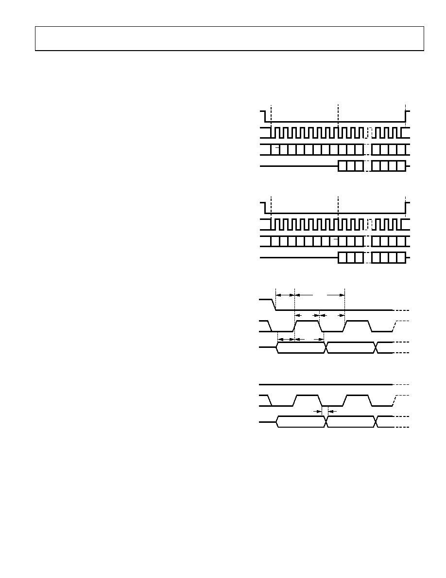
SERIAL INTERFACE PORT PIN DESCRIPTIONS
Serial Clock (SCLK)
The serial clock pin synchronizes data to and from the device
and controls the internal state machines. The maximum frequency
of SCLK is 40 MHz. All data input is registered on the rising edge
of SCLK. All data is driven out on the falling edge of SCLK.
Chip Select (CSB)
Active low input starts and gates a communication cycle. It
allows more than one device to be used on the same serial
communication lines. The SDO and SDIO pins go to a high
impedance state when this input is high. Chip select should
stay low during the entire communication cycle.
Serial Data I/O (SDIO)
Data is always written into the device on this pin. However, this
pin can be used as a bidirectional data line. The configuration
of this pin is controlled by Register 0x00, Bit 7. The default is
Logic 0, configuring the SDIO pin as unidirectional.
Serial Data Out (SDO)
Data is read from this pin for protocols that use separate lines
for transmitting and receiving data. In the case where the device
operates in a single bidirectional I/O mode, this pin does not
output data and is set to a high impedance state.
MSB/LSB TRANSFERS
The serial port can support both MSB-first and LSB-first data
formats. This functionality is controlled by the LSB-/MSB-first
register bit (Register 0x00, Bit 6). The default is MSB-first format
(LSB/MSB first = 0).
When MSB-first format is selected (LSB/MSB first = 0), the
instruction and data bit must be written from MSB to LSB.
Multibyte data transfers in MSB-first format start with an
instruction byte that includes the register address of the most
significant data byte. Subsequent data bytes should follow from
high address to low address. In MSB-first mode, the serial port
internal byte address generator decrements for each data byte of
the multibyte communication cycle.
When LSB/MSB first = 1 (LSB first) the instruction and data
bit must be written from LSB to MSB. Multibyte data transfers
in LSB-first format start with an instruction byte that includes
the register address of the least significant data byte, followed by
multiple data bytes. The serial port internal byte address genera-
tor increments for each byte of the multibyte communication cycle.
The serial port controller data address decrements from the data
address written toward 0x00 for multibyte I/O operations if the
MSB-first format is active. The serial port controller address
increments from the data address written toward 0x1F for
multibyte I/O operations if the LSB-first format is active.
R/W N1 N0 A4 A3
A2 A1 A0 D7 D6N D5N
D00
D10
D20
D30
D7 D6N D5N
D00
D10
D20
D30
INSTRUCTION CYCLE
DATA TRANSFER CYCLE
CSB
SCLK
SDIO
SDO
06
45
2-
05
0
Figure 53. Serial Register Interface Timing, MSB First
A0 A1 A2 A3 A4
N0 N1 R/W D00 D10 D20
D7N
D6N
D5N
D4N
D00 D10 D20
D7N
D6N
D5N
D4N
INSTRUCTION CYCLE
DATA TRANSFER CYCLE
CSB
SCLK
SDIO
SDO
06
45
2-
05
1
Figure 54. Serial Register Interface Timing, LSB First
INSTRUCTION BIT 6
INSTRUCTION BIT 7
CSB
SCLK
SDIO
tDS
tDH
tPWH
tPWL
tSCLK
06
45
2-
05
2
Figure 55. Timing Diagram for 3-Wire Interface Register Write
DATA BIT n – 1
DATA BIT n
CSB
SCLK
SDIO
SDO
tDV
0
64
52
-0
53
Figure 56. Timing Diagram for 3-Wire Interface Register Read
相关PDF资料 |
PDF描述 |
|---|---|
| SDR0403-101KL | INDUCTOR 100UH 10% NON-SHLD SMD |
| AD9776A-DPG2-EBZ | BOARD EVALUATION FOR AD9776A |
| DC1009A-B | BOARD DELTA SIGMA ADC LTC2488 |
| AD9787-DPG2-EBZ | BOARD EVALUATION FOR AD9787 |
| ESA10DTKS | CONN EDGECARD 20POS DIP .125 SLD |
相关代理商/技术参数 |
参数描述 |
|---|---|
| AD9778A-EBZ | 制造商:Analog Devices 功能描述:Dual 12 /14 /16 Bit, 1 GSPS, Digital To Analog Converters Development Kit 制造商:Analog Devices 功能描述:DUAL 14B, 1.0 GSPS TXDAC - Bulk |
| AD9778BSVZ | 功能描述:IC DAC 14BIT DUAL 1GSPS 100TQFP RoHS:是 类别:集成电路 (IC) >> 数据采集 - 数模转换器 系列:- 产品培训模块:Lead (SnPb) Finish for COTS Obsolescence Mitigation Program 标准包装:1,000 系列:- 设置时间:1µs 位数:8 数据接口:串行 转换器数目:8 电压电源:双 ± 功率耗散(最大):941mW 工作温度:0°C ~ 70°C 安装类型:表面贴装 封装/外壳:24-SOIC(0.295",7.50mm 宽) 供应商设备封装:24-SOIC W 包装:带卷 (TR) 输出数目和类型:8 电压,单极 采样率(每秒):* |
| AD9778BSVZ1 | 制造商:AD 制造商全称:Analog Devices 功能描述:Dual 12-/14-/16-Bit, 1 GSPS, Digital-to-Analog Converters |
| AD9778BSVZRL | 功能描述:IC DAC 14BIT DUAL 1GSPS 100TQFP RoHS:是 类别:集成电路 (IC) >> 数据采集 - 数模转换器 系列:- 产品培训模块:Data Converter Fundamentals DAC Architectures 标准包装:750 系列:- 设置时间:7µs 位数:16 数据接口:并联 转换器数目:1 电压电源:双 ± 功率耗散(最大):100mW 工作温度:0°C ~ 70°C 安装类型:表面贴装 封装/外壳:28-LCC(J 形引线) 供应商设备封装:28-PLCC(11.51x11.51) 包装:带卷 (TR) 输出数目和类型:1 电压,单极;1 电压,双极 采样率(每秒):143k |
| AD9778BSVZRL1 | 制造商:AD 制造商全称:Analog Devices 功能描述:Dual 12-/14-/16-Bit, 1 GSPS, Digital-to-Analog Converters |
发布紧急采购,3分钟左右您将得到回复。