- 您现在的位置:买卖IC网 > PDF目录17064 > AD9778A-DPG2-EBZ (Analog Devices Inc)BOARD EVALUATION FOR AD9778A PDF资料下载
参数资料
| 型号: | AD9778A-DPG2-EBZ |
| 厂商: | Analog Devices Inc |
| 文件页数: | 44/56页 |
| 文件大小: | 0K |
| 描述: | BOARD EVALUATION FOR AD9778A |
| 标准包装: | 1 |
| 系列: | * |
| DAC 的数量: | 2 |
| 位数: | 14 |
| 采样率(每秒): | 1G |
| 数据接口: | 并联 |
| DAC 型: | 电流 |
| 工作温度: | -40°C ~ 85°C |
| 已供物品: | * |
| 已用 IC / 零件: | AD9778A |
第1页第2页第3页第4页第5页第6页第7页第8页第9页第10页第11页第12页第13页第14页第15页第16页第17页第18页第19页第20页第21页第22页第23页第24页第25页第26页第27页第28页第29页第30页第31页第32页第33页第34页第35页第36页第37页第38页第39页第40页第41页第42页第43页当前第44页第45页第46页第47页第48页第49页第50页第51页第52页第53页第54页第55页第56页
AD9776A/AD9778A/AD9779A
Rev. B | Page 49 of 56
DEVICE SYNCHRONIZATION
System demands can impose two different requirements for
synchronization. Some systems require multiple DACs to be
synchronized to each other. This is the case when supporting
transmit diversity or beam forming, where multiple antennas
are used to transmit a correlated signal. In this case, the DAC
outputs need to be phase aligned with each other, but there may
not be a requirement for the DAC outputs to be aligned with a
system level reference clock. In systems with a time division
multiplexing transmit chain, one or more DACs may need to be
synchronized with a system level reference clock. The options
for synchronizing devices under these two conditions are
described in the Synchronization Logic Overview section
and the Synchronizing Devices to a System Clock section.
SYNCHRONIZATION LOGIC OVERVIEW
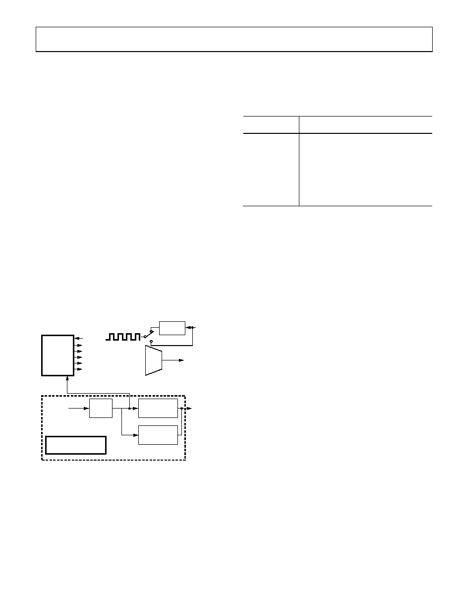
Figure 88 shows the block diagram of the on-chip synchroniza-
tion logic. The basic operation of the synchronization logic is to
generate a single DACCLK-cycle-wide initialization pulse that
sets the clock generation state machine logic to a known state.
This initialization pulse loads the clock generation state machine
with the Clock State[4:0] value as its next state. If the initializa-
tion pulse from the synchronization logic is generated properly,
it is active for one DACCLK cycle, every 32 DACCLK cycles.
Because the clock generation state machine has 32 states operating
at the DACCLK rate, every initialization pulse received after the
first pulse loads the state in which the state machine is already
in, maintaining proper clocking operation of the device.
SYNC
DELAY
PULSE
GENERATION
LOGIC
ERROR DETECT
CIRCUITRY
CLOCK
GENERATION
STATE
MACHINE
DACCLK
BIT 0 (1× INTERPOLATION)
BIT 1 (2×)
BIT 2 (4×)
BIT 3 (8×)
BIT 4 (8× WITH
ZERO STUFFING)
MUX
SYNC IRQ
SYNC_I
DELAY REGISTER
(REG 0x0, BITS[7:4])
REFCLK
INTERNAL
PLL
BYPASS
06
45
2-
0
94
LOAD DACCLK OFFSET VALUE (REG 0x07,
BITS[4:0]), ONE DACCLK CYCLE/INCREMENT
fSYNC_1 < fDATA/2^N
Figure 88. Synchronization Circuitry Block Diagram
Nominally, the SYNC_I input should have one rising edge every
32 clock cycles (or multiple of 32 clock cycles) to maintain
proper synchronization. The pulse generation logic can be
programmed to suppress outgoing pulses if the incoming
SYNC_I frequency is greater than DACCLK/32. Extra pulses
can be suppressed by the ratios listed in Table 30. The SYNC_I
frequency can be lower than DACCLK/32 as long as output
pulses are generated from the pulse generation circuit on a
multiple of 32 DACCLK periods. In any case, the maximum
frequency of SYNC_I must be less than fDATACLK.
Table 30. Settings Required to Support Various SYNC_I
Frequencies
SYNC_I
Ratio[2:0]
SYNC_I Rising Edges Required for
Synchronization Pulse
000
1 (default)
001
2
010
4
011
8
100
16
101
Invalid setting
110
Invalid setting
111
Invalid setting
As an example, if a SYNC_I signal with a frequency of fDACCLK/4
is used, then both 011 and 100 are valid settings for the SYNC_I
Ratio[2:0] value. A setting of 011 results in one initialization
pulse being generated every 32 DACCLK cycles, and a setting
of 100 results in one initialization pulse being generated every
64 DACCLK cycles. Both cases result in proper device
synchronization.
The Clock State[4:0] value is the state to which the clock
generation state machine resets upon initialization. By varying
this value, the timing of the internal clocks with respect to the
SYNC_I signal can be adjusted. Every increment of the Clock
State[4:0] value advances the internal clocks by one DACCLK
period.
Synchronization Timing Error Detection
The synchronization logic has error detection circuitry similar to
the input data timing. The SYNC_I Timing Margin[3:0] variable
determines how much setup and hold margin the synchronization
interface needs for the sync timing error IRQ bit to remain inactive
(that is, to indicate error free operation). Therefore, the sync timing
error IRQ bit is set whenever the setup and hold margins drop
below the SYNC_I Timing Margin[3:0] value and, therefore,
does not necessarily indicate that the SYNC_I input was latched
incorrectly.
When the sync timing error IRQ bit is set, corrective action can
be taken to restore timing margin. One course of action is to
temporarily reduce the timing margin until the sync timing
error IRQ is cleared. Then, increase the SYNC_I delay by two
increments and check whether the timing margin has increased
or decreased. If it has increased, continue incrementing the
value of SYNC_I delay until the margin is maximized. However,
if incrementing the SYNC_I delay reduced the timing margin,
then the delay should be reduced until the timing margin is
optimized.
相关PDF资料 |
PDF描述 |
|---|---|
| SDR0403-101KL | INDUCTOR 100UH 10% NON-SHLD SMD |
| AD9776A-DPG2-EBZ | BOARD EVALUATION FOR AD9776A |
| DC1009A-B | BOARD DELTA SIGMA ADC LTC2488 |
| AD9787-DPG2-EBZ | BOARD EVALUATION FOR AD9787 |
| ESA10DTKS | CONN EDGECARD 20POS DIP .125 SLD |
相关代理商/技术参数 |
参数描述 |
|---|---|
| AD9778A-EBZ | 制造商:Analog Devices 功能描述:Dual 12 /14 /16 Bit, 1 GSPS, Digital To Analog Converters Development Kit 制造商:Analog Devices 功能描述:DUAL 14B, 1.0 GSPS TXDAC - Bulk |
| AD9778BSVZ | 功能描述:IC DAC 14BIT DUAL 1GSPS 100TQFP RoHS:是 类别:集成电路 (IC) >> 数据采集 - 数模转换器 系列:- 产品培训模块:Lead (SnPb) Finish for COTS Obsolescence Mitigation Program 标准包装:1,000 系列:- 设置时间:1µs 位数:8 数据接口:串行 转换器数目:8 电压电源:双 ± 功率耗散(最大):941mW 工作温度:0°C ~ 70°C 安装类型:表面贴装 封装/外壳:24-SOIC(0.295",7.50mm 宽) 供应商设备封装:24-SOIC W 包装:带卷 (TR) 输出数目和类型:8 电压,单极 采样率(每秒):* |
| AD9778BSVZ1 | 制造商:AD 制造商全称:Analog Devices 功能描述:Dual 12-/14-/16-Bit, 1 GSPS, Digital-to-Analog Converters |
| AD9778BSVZRL | 功能描述:IC DAC 14BIT DUAL 1GSPS 100TQFP RoHS:是 类别:集成电路 (IC) >> 数据采集 - 数模转换器 系列:- 产品培训模块:Data Converter Fundamentals DAC Architectures 标准包装:750 系列:- 设置时间:7µs 位数:16 数据接口:并联 转换器数目:1 电压电源:双 ± 功率耗散(最大):100mW 工作温度:0°C ~ 70°C 安装类型:表面贴装 封装/外壳:28-LCC(J 形引线) 供应商设备封装:28-PLCC(11.51x11.51) 包装:带卷 (TR) 输出数目和类型:1 电压,单极;1 电压,双极 采样率(每秒):143k |
| AD9778BSVZRL1 | 制造商:AD 制造商全称:Analog Devices 功能描述:Dual 12-/14-/16-Bit, 1 GSPS, Digital-to-Analog Converters |
发布紧急采购,3分钟左右您将得到回复。