参数资料
| 型号: | AD9779ABSVZRL |
| 厂商: | Analog Devices Inc |
| 文件页数: | 42/56页 |
| 文件大小: | 0K |
| 描述: | DAC 16BIT 1.0GSPS 100-TQFP |
| 产品培训模块: | Data Converter Fundamentals DAC Architectures |
| 设计资源: | Interfacing ADL5370 to AD9779A Dual-Channel, 1 GSPS High Speed DAC (CN0016) Interfacing ADL5371 to AD9779A Dual-Channel, 1 GSPS High Speed DAC (CN0017) Interfacing ADL5372 to AD9779A Dual-Channel, 1 GSPS High Speed DAC (CN0018) Interfacing ADL5373 to AD9779A Dual-Channel, 1 GSPS High Speed DAC (CN0019) Interfacing ADL5374 to AD9779A Dual-Channel, 1 GSPS High Speed DAC (CN0020) Interfacing ADL5375 to AD9779A Dual-Channel, 1 GSPS High Speed DAC (CN0021) |
| 标准包装: | 1,000 |
| 位数: | 16 |
| 数据接口: | 串行 |
| 转换器数目: | 2 |
| 电压电源: | 模拟和数字 |
| 功率耗散(最大): | 300mW |
| 工作温度: | -40°C ~ 85°C |
| 安装类型: | 表面贴装 |
| 封装/外壳: | 100-TQFP 裸露焊盘 |
| 供应商设备封装: | 100-TQFP-EP(14x14) |
| 包装: | 带卷 (TR) |
| 输出数目和类型: | 4 电流,单极 |
| 采样率(每秒): | 1G |
第1页第2页第3页第4页第5页第6页第7页第8页第9页第10页第11页第12页第13页第14页第15页第16页第17页第18页第19页第20页第21页第22页第23页第24页第25页第26页第27页第28页第29页第30页第31页第32页第33页第34页第35页第36页第37页第38页第39页第40页第41页当前第42页第43页第44页第45页第46页第47页第48页第49页第50页第51页第52页第53页第54页第55页第56页
AD9776A/AD9778A/AD9779A
Rev. B | Page 47 of 56
The DATACLKDIV only affects the DATACLK output frequency,
not the frequency of the data sampling clock. To maintain an
fDATACLK frequency that samples the input data that remains
consistent with the expected data rate, DATACLKDIV should
be set to 00.
Table 27. DACCLK to DATACLK Divisor Values
Variable
Value
Address
Register
Bit
IF
Interpolation factor (1, 2, 4,
or 8)
0x01
[7:6]
ZS
1, if zero stuffing is disabled
2, if zero stuffing is enabled
0x01
[0]
SP
0.5, if single port is enabled
1, if dual port is selected
0x02
[6]
DATACLKDIV
1, 2, or 4
0x03
[5:4]
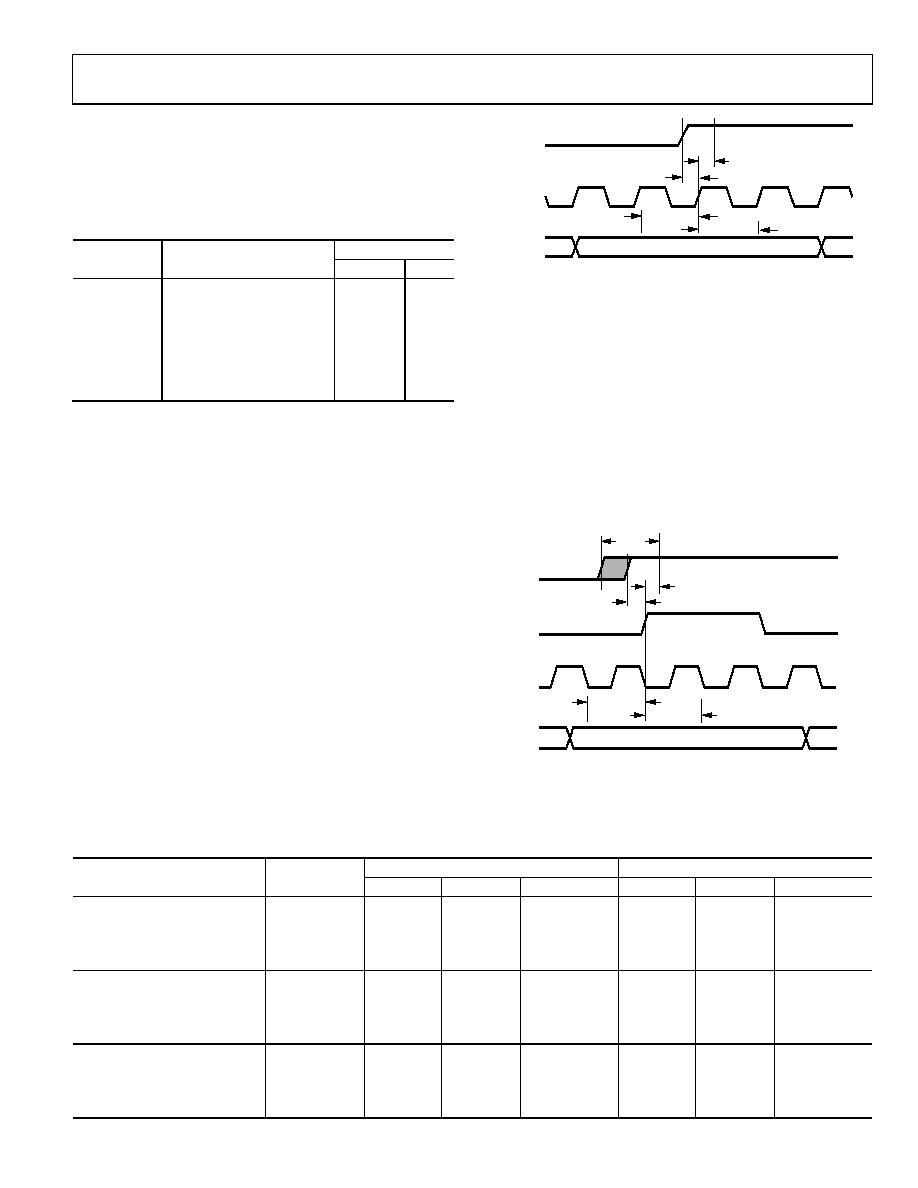
INPUT DATA REFERENCED TO REFCLK
In some systems, it may be more convenient to use the REFCLK
input than the DATACLK output as the input data timing
reference. If the frequency of DACCLK is equal to the frequency
of the data input (without interpolation), then the data with
respect to REFCLK± timing specifications in Table 28 apply
directly without further considerations. If the frequency of
DACCLK is greater than the frequency of the input data, a
divider is used to generate the DATACLK output (and the
internal data sampling clock). This divider creates a phase
ambiguity between REFCLK and DATACLK, which results in
uncertainty in the sampling time. To establish fixed setup and
hold times of the data interface, this phase ambiguity must be
eliminated.
To eliminate the phase ambiguity, the SYNC_I input pins (Pin 13
and Pin 14) must be used to force the data to be sampled on a
specific REFCLK edge. The relationship among REFCLK,
Therefore, both SYNC_I and data must meet the timing in
Table 28 for reliable data transfer into the device.
06
452
-30
9
tSREFCLK
tHREFCLK
tS_SYNC
tH_SYNC
SYNC_I
REFCLK
DATA
Figure 84. Input Data Port Timing, Data Referenced to REFCLK, fDACCLK = fREFCLK
Note that even though the setup and hold times of SYNC_I
are relative to REFCLK, the SYNC_I input is sampled at the
internal DACCLK rate. In the case where the PLL is employed,
SYNC_I must be asserted to meet the setup time with respect to
REFCLK (tS_SYNC), but cannot be asserted prior to the previous
rising edge of the internal SYNC_I sample clock. In other words,
the SYNC_I assert edge has to be placed between its successive
keep out windows that replicate at the DACCLK rate, not the
REFCLK rate. The valid window for asserting SYNC_I is
shaded gray in Figure 85 for the case where the PLL provides a
DACCLK frequency of four times the REFCLK frequency.
Thus, the minimum setup time is tS_SYNC, and the maximum
setup time is tDACCLK tH_SYNC.
tSREFCLK
tDACCLK
tH_SYNC
tS_SYNC
tHREFCLK
06
45
2-
31
0
DACCLK
DATA
SYNC_I
REFCLK
Figure 85. Input Data Port Timing, Data Referenced to REFCLK,
fDACCLK = fREFCLK × 4
More details of the synchronization circuitry are found in the
Device Synchronization section of this data sheet.
Table 28. Data Timing Specifications vs. Temperature
Timing Parameter
Temperature
PLL Disabled
PLL Enabled
Min tS (ns)
Min tH (ns)
Min KOW (ns)
Min tS (ns)
Min tH (ns)
Min KOW (ns)
Data with Respect to REFCLK±
40°C
0.80
3.35
2.55
0.83
3.87
2.99
+25°C
1.00
3.50
2.50
1.06
4.04
2.98
+85°C
1.10
3.80
2.70
1.19
4.37
3.16
40°C to +85°C
0.80
3.80
3.00
0.83
4.37
3.54
Data with Respect to DATACLK
40°C
2.50
0.05
2.45
2.50
0.05
2.45
+25°C
2.70
0.20
2.50
2.70
0.20
2.50
+85°C
3.00
0.40
2.60
3.00
0.40
2.60
40°C to +85°C
3.00
0.05
2.95
3.00
0.05
2.95
SYNC_I± to REFCLK±
40°C
0.30
0.65
0.95
0.27
1.17
1.39
+25°C
0.25
0.75
1.00
0.19
1.29
1.48
+85°C
0.15
0.90
1.05
0.06
1.47
1.51
40°C to +85°C
0.30
0.90
1.20
0.27
1.47
1.74
相关PDF资料 |
PDF描述 |
|---|---|
| AD977ABNZ | IC ADC 16BIT 200KSPS 20DIP |
| AD9781BCPZ | IC DAC 14BT 500MSPS LVDS 72LFCSP |
| AD9877ABSZ | IC PROCESSOR FRONT END 100MQFP |
| AD9878BSTZ | IC FRONT-END MIXED-SGNL 100-LQFP |
| AD9879BSZ | IC PROCESSOR FRONT END 100MQFP |
相关代理商/技术参数 |
参数描述 |
|---|---|
| AD9779A-DPG2-EBZ | 功能描述:BOARD EVALUATION FOR AD9779A RoHS:是 类别:编程器,开发系统 >> 评估板 - 数模转换器 (DAC) 系列:* 产品培训模块:Lead (SnPb) Finish for COTS Obsolescence Mitigation Program 标准包装:1 系列:- DAC 的数量:4 位数:12 采样率(每秒):- 数据接口:串行,SPI? 设置时间:3µs DAC 型:电流/电压 工作温度:-40°C ~ 85°C 已供物品:板 已用 IC / 零件:MAX5581 |
| AD9779A-EBZ | 制造商:Analog Devices 功能描述:DUAL 16B, 1.0 GSPS TXDAC - Bulk |
| AD9779AMOD-EBZ | 制造商:Analog Devices 功能描述:DUAL 16B, 1.0 GSPS TXDAC - Bulk |
| AD9779AXSVZ | 制造商:Analog Devices 功能描述:DUAL 16-BIT, 1 GSPS, DIGITAL-TO-ANALOG CONVERTER - Bulk |
| AD9779BSV | 制造商:Analog Devices 功能描述:DAC 2CH INTERPOLATION FLTR 16BIT 100TQFP EP - Bulk |
发布紧急采购,3分钟左右您将得到回复。