- 您现在的位置:买卖IC网 > PDF目录10979 > AD9852ASTZ (Analog Devices Inc)IC DDS SYNTHESIZER CMOS 80-LQFP PDF资料下载
参数资料
| 型号: | AD9852ASTZ |
| 厂商: | Analog Devices Inc |
| 文件页数: | 20/52页 |
| 文件大小: | 0K |
| 描述: | IC DDS SYNTHESIZER CMOS 80-LQFP |
| 产品培训模块: | Direct Digital Synthesis Tutorial Series (1 of 7): Introduction Direct Digital Synthesizer Tutorial Series (7 of 7): DDS in Action Direct Digital Synthesis Tutorial Series (3 of 7): Angle to Amplitude Converter Direct Digital Synthesis Tutorial Series (6 of 7): SINC Envelope Correction Direct Digital Synthesis Tutorial Series (4 of 7): Digital-to-Analog Converter Direct Digital Synthesis Tutorial Series (2 of 7): The Accumulator |
| 标准包装: | 1 |
| 分辨率(位): | 12 b |
| 主 fclk: | 200MHz |
| 调节字宽(位): | 48 b |
| 电源电压: | 3.14 V ~ 3.47 V |
| 工作温度: | -40°C ~ 85°C |
| 安装类型: | 表面贴装 |
| 封装/外壳: | 80-LQFP |
| 供应商设备封装: | 80-LQFP(14x14) |
| 包装: | 托盘 |
| 产品目录页面: | 552 (CN2011-ZH PDF) |
| 配用: | AD9852/PCBZ-ND - BOARD EVAL FOR AD9852 |
第1页第2页第3页第4页第5页第6页第7页第8页第9页第10页第11页第12页第13页第14页第15页第16页第17页第18页第19页当前第20页第21页第22页第23页第24页第25页第26页第27页第28页第29页第30页第31页第32页第33页第34页第35页第36页第37页第38页第39页第40页第41页第42页第43页第44页第45页第46页第47页第48页第49页第50页第51页第52页
AD9852
Rev. E | Page 27 of 52
USING THE AD9852
INTERNAL AND EXTERNAL UPDATE CLOCK
The update clock function is composed of a bidirectional
I/O pin (Pin 20) and a programmable 32-bit down-counter. In
order for programming changes to be transferred from the I/O
buffer registers to the active core of the DDS, a clock signal
(low-to-high edge) must be externally supplied to Pin 20 or
internally generated by the 32-bit update clock.
When the user provides an external update clock, it is internally
synchronized with the system clock to prevent partial transfer
of program register information due to violation of data setup
or hold times. This mode provides the user with complete control
of when updated program information becomes effective. The
default mode for the update clock is internal (internal/external
update clock control register bit is logic high). To switch to
external update clock mode, the internal/external update clock
control register bit must be set to logic low. The internal update
mode generates automatic, periodic update pulses at intervals
set by the user.
An internally generated update clock can be established by
programming the 32-bit update clock registers (Address 16 hex
to Address 19 hex) and setting the internal/external update clock
control register bit (Address 1F hex) to logic high. The update
clock countdown counter function operates at half the rate of
the system clock (150 MHz maximum) and counts down from a
32-bit binary value (programmed by the user). When the count
reaches 0, an automatic I/O update of the DDS output or the DDS
functions is generated. The update clock is internally and externally
routed to Pin 20 to allow users to synchronize the programming of
update information with the update clock rate. The time between
update pulses is given as
(N + 1)(System Clock Period × 2)
where N is the 32-bit value programmed by the user, and the
allowable range of N is from 1 to (232 1).
The internally generated update pulse output on Pin 20 has a
fixed high time of eight system clock cycles.
Programming the update clock register for values less than 5 causes
the I/O UD CLK pin to remain high. Although the update clock
can still function in this state, it cannot be used to indicate when
data is transferring. This is an effect of the minimum high pulse
time when I/O UD CLK functions as an output.
ON/OFF OUTPUT SHAPED KEYING (OSK)
The on/off OSK feature allows the user to control the amplitude
vs. time slope of the cosine DAC output signal. This function is
used in burst transmissions of digital data to reduce the adverse
spectral impact of short, abrupt bursts of data. Users must first
enable the digital multiplier by setting the OSK EN bit (Control
Register Address 20 hex) to logic high in the control register.
Otherwise, if the OSK EN bit is set low, the digital multiplier
responsible for amplitude control is bypassed, and the cosine
DAC output is set to full-scale amplitude.
In addition to setting the OSK EN bit, a second control bit, OSK
INT (also at Address 20 hex), must be set to logic high. Logic high
selects the linear internal control of the output ramp-up or ramp-
down function. A logic low in the OSK INT bit switches control
of the digital multiplier to a user-programmable 12-bit register,
allowing users to dynamically shape the amplitude transition in
practically any fashion. The 12-bit register, labeled output shape
key, is located at Address 21 hex to Address 22 hex, as indicated
in Table 9. The maximum output amplitude is a function of the
RSET resistor and is not programmable when OSK INT is enabled.
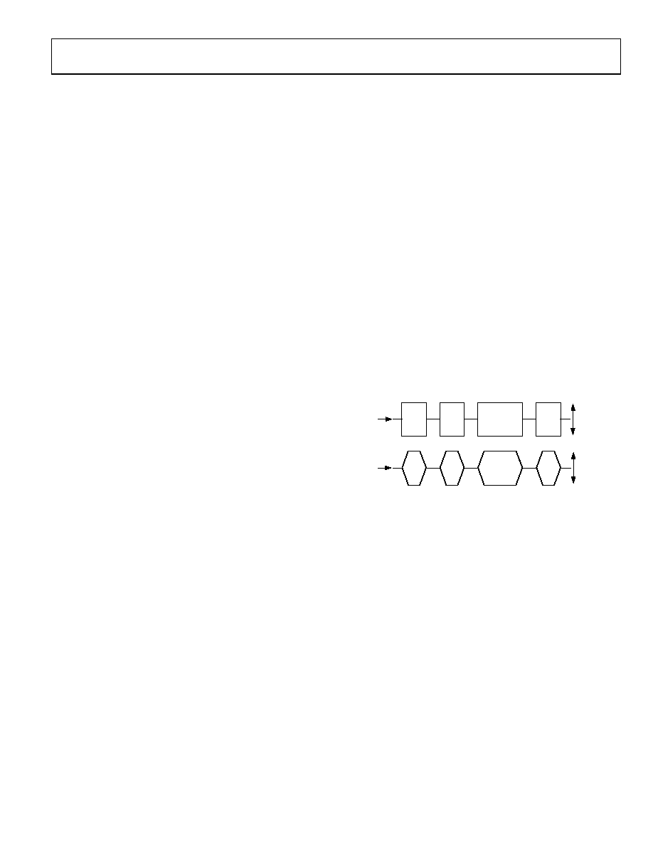
ABRUPT ON/OFF KEYING
SHAPED ON/OFF KEYING
ZERO
SCALE
ZERO
SCALE
FULL
SCALE
FULL
SCALE
00634-046
Figure 46. On/Off Output Shaped Keying
The transition time from zero scale to full scale must also be
programmed. The transition time is a function of two fixed
elements and one variable. The variable element is the pro-
grammable 8-bit ramp rate counter. This is a countdown counter
that is clocked at the system clock rate (300 MHz maximum)
and generates one pulse whenever the counter reaches 0. This
pulse is routed to a 12-bit counter that increments with each
pulse received. The outputs of the 12-bit counter are connected
to the 12-bit digital multiplier. When the digital multiplier has
a value of all 0s at its inputs, the input signal is multiplied by 0,
producing zero scale. When the multiplier has a value of all 1s,
the input signal is multiplied by a value of 4095 or 4096, producing
nearly full scale. There are 4094 remaining fractional multiplier
values that produce output amplitudes scaled according to their
binary values.
相关PDF资料 |
PDF描述 |
|---|---|
| VE-2WY-IY-F4 | CONVERTER MOD DC/DC 3.3V 33W |
| VE-2WY-IX-F3 | CONVERTER MOD DC/DC 3.3V 49.5W |
| AD9953YSVZ | IC DDS DAC 14BIT 400MSPS 48-TQFP |
| VE-2WX-IY-F4 | CONVERTER MOD DC/DC 5.2V 50W |
| DS3174+ | IC TXRX DS3/E3 QUAD 400-BGA |
相关代理商/技术参数 |
参数描述 |
|---|---|
| AD9852ASTZ | 制造商:Analog Devices 功能描述:IC DDS 100MHZ LQFP-80 |
| AD9852ASTZ1 | 制造商:AD 制造商全称:Analog Devices 功能描述:CMOS 300 MSPS Complete DDS |
| AD9852ASVZ | 功能描述:IC DDS SYNTHESIZER CMOS 80-TQFP RoHS:是 类别:集成电路 (IC) >> 接口 - 直接数字合成 (DDS) 系列:- 产品变化通告:Product Discontinuance 27/Oct/2011 标准包装:2,500 系列:- 分辨率(位):10 b 主 fclk:25MHz 调节字宽(位):32 b 电源电压:2.97 V ~ 5.5 V 工作温度:-40°C ~ 85°C 安装类型:表面贴装 封装/外壳:16-TSSOP(0.173",4.40mm 宽) 供应商设备封装:16-TSSOP 包装:带卷 (TR) |
| AD9852ASVZ | 制造商:Analog Devices 功能描述:IC DDS 300MHz TQFP-80 制造商:Analog Devices 功能描述:IC, DDS, 300MHz, TQFP-80 |
| AD9852ASVZ1 | 制造商:AD 制造商全称:Analog Devices 功能描述:CMOS 300 MSPS Complete DDS |
发布紧急采购,3分钟左右您将得到回复。