- 您现在的位置:买卖IC网 > PDF目录10979 > AD9852ASTZ (Analog Devices Inc)IC DDS SYNTHESIZER CMOS 80-LQFP PDF资料下载
参数资料
| 型号: | AD9852ASTZ |
| 厂商: | Analog Devices Inc |
| 文件页数: | 21/52页 |
| 文件大小: | 0K |
| 描述: | IC DDS SYNTHESIZER CMOS 80-LQFP |
| 产品培训模块: | Direct Digital Synthesis Tutorial Series (1 of 7): Introduction Direct Digital Synthesizer Tutorial Series (7 of 7): DDS in Action Direct Digital Synthesis Tutorial Series (3 of 7): Angle to Amplitude Converter Direct Digital Synthesis Tutorial Series (6 of 7): SINC Envelope Correction Direct Digital Synthesis Tutorial Series (4 of 7): Digital-to-Analog Converter Direct Digital Synthesis Tutorial Series (2 of 7): The Accumulator |
| 标准包装: | 1 |
| 分辨率(位): | 12 b |
| 主 fclk: | 200MHz |
| 调节字宽(位): | 48 b |
| 电源电压: | 3.14 V ~ 3.47 V |
| 工作温度: | -40°C ~ 85°C |
| 安装类型: | 表面贴装 |
| 封装/外壳: | 80-LQFP |
| 供应商设备封装: | 80-LQFP(14x14) |
| 包装: | 托盘 |
| 产品目录页面: | 552 (CN2011-ZH PDF) |
| 配用: | AD9852/PCBZ-ND - BOARD EVAL FOR AD9852 |
第1页第2页第3页第4页第5页第6页第7页第8页第9页第10页第11页第12页第13页第14页第15页第16页第17页第18页第19页第20页当前第21页第22页第23页第24页第25页第26页第27页第28页第29页第30页第31页第32页第33页第34页第35页第36页第37页第38页第39页第40页第41页第42页第43页第44页第45页第46页第47页第48页第49页第50页第51页第52页
AD9852
Rev. E | Page 28 of 52
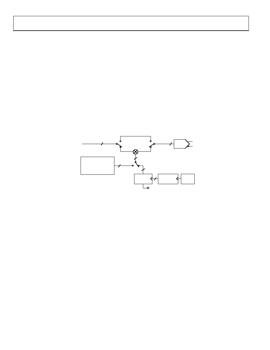
The two fixed elements of the transition time are the period of
the system clock (which drives the ramp rate counter) and the
number of amplitude steps (4096). For example, if the system
clock of the AD9852 is 100 MHz (10 ns period) and the ramp
rate counter is programmed for a minimum count of 3, two system
clock periods are required: one rising edge loads the countdown
value, and the next edge decrements the counter from 3 to 2. If the
countdown value is less than 3, the ramp rate counter stalls and
therefore produces a constant scaling value to the digital multiplier.
This stall condition may have an application for the user.
The relationship of the 8-bit countdown value to the time between
output pulses is given as
(N + 1) × System Clock Period
where N is the 8-bit countdown value.
A total of 4096 output pulses is required to advance the 12-bit
up-counter from zero scale to full scale. Therefore, the minimum
output shaped keying ramp time for a 100 MHz system clock is
4096 × 4 × 10 ns ≈ 164 μs
The maximum ramp time is
4096 × 256 × 10 ns ≈ 10.5 ms
Finally, by changing the logic state of Pin 30, output shaped
keying automatically performs the programmed output envelope
functions when OSK INT is high. A logic high on Pin 30 causes
the outputs to linearly ramp up to full-scale amplitude and hold
until the logic level is changed to low, causing the outputs to
ramp down to zero scale.
12-BIT DIGITAL
MULTIPLIER
12
(BYPASS MULTIPLIER)
OSK EN = 0
OSK EN = 1
OSK EN = 0
OSK EN = 1
12
DIGITAL
SIGNAL IN
USER-PROGRAMMABLE
12-BIT MULTIPLIER
OUTPUT SHAPED
KEYING MULTIPLIER
REGISTER
12
OSK INT = 1
OSK INT = 0
1
8-BIT RAMP
RATE
COUNTER
SYSTEM
CLOCK
ON/OFF OUTPUT SHAPED
KEYING PIN
12-BIT
UP/DOWN
COUNTER
DDS DIGITAL
OUTPUT
COSINE
DAC
00634-047
Figure 47. Block Diagram of the Digital Multiplier Section Responsible for the Output Shaped Keying Function
相关PDF资料 |
PDF描述 |
|---|---|
| VE-2WY-IY-F4 | CONVERTER MOD DC/DC 3.3V 33W |
| VE-2WY-IX-F3 | CONVERTER MOD DC/DC 3.3V 49.5W |
| AD9953YSVZ | IC DDS DAC 14BIT 400MSPS 48-TQFP |
| VE-2WX-IY-F4 | CONVERTER MOD DC/DC 5.2V 50W |
| DS3174+ | IC TXRX DS3/E3 QUAD 400-BGA |
相关代理商/技术参数 |
参数描述 |
|---|---|
| AD9852ASTZ | 制造商:Analog Devices 功能描述:IC DDS 100MHZ LQFP-80 |
| AD9852ASTZ1 | 制造商:AD 制造商全称:Analog Devices 功能描述:CMOS 300 MSPS Complete DDS |
| AD9852ASVZ | 功能描述:IC DDS SYNTHESIZER CMOS 80-TQFP RoHS:是 类别:集成电路 (IC) >> 接口 - 直接数字合成 (DDS) 系列:- 产品变化通告:Product Discontinuance 27/Oct/2011 标准包装:2,500 系列:- 分辨率(位):10 b 主 fclk:25MHz 调节字宽(位):32 b 电源电压:2.97 V ~ 5.5 V 工作温度:-40°C ~ 85°C 安装类型:表面贴装 封装/外壳:16-TSSOP(0.173",4.40mm 宽) 供应商设备封装:16-TSSOP 包装:带卷 (TR) |
| AD9852ASVZ | 制造商:Analog Devices 功能描述:IC DDS 300MHz TQFP-80 制造商:Analog Devices 功能描述:IC, DDS, 300MHz, TQFP-80 |
| AD9852ASVZ1 | 制造商:AD 制造商全称:Analog Devices 功能描述:CMOS 300 MSPS Complete DDS |
发布紧急采购,3分钟左右您将得到回复。