- 您现在的位置:买卖IC网 > PDF目录10979 > AD9910BSVZ (Analog Devices Inc)IC DDS 1GSPS 14BIT PAR 100TQFP PDF资料下载
参数资料
| 型号: | AD9910BSVZ |
| 厂商: | Analog Devices Inc |
| 文件页数: | 16/64页 |
| 文件大小: | 0K |
| 描述: | IC DDS 1GSPS 14BIT PAR 100TQFP |
| 产品培训模块: | Direct Digital Synthesis Tutorial Series (1 of 7): Introduction Direct Digital Synthesizer Tutorial Series (7 of 7): DDS in Action Direct Digital Synthesis Tutorial Series (3 of 7): Angle to Amplitude Converter Direct Digital Synthesis Tutorial Series (6 of 7): SINC Envelope Correction Direct Digital Synthesis Tutorial Series (4 of 7): Digital-to-Analog Converter Direct Digital Synthesis Tutorial Series (2 of 7): The Accumulator |
| 设计资源: | Synchronizing Multiple AD9910 1 GSPS Direct Digital Synthesizers (CN0121) |
| 标准包装: | 1 |
| 分辨率(位): | 14 b |
| 主 fclk: | 1GHz |
| 调节字宽(位): | 32 b |
| 电源电压: | 1.8V, 3.3V |
| 工作温度: | -40°C ~ 85°C |
| 安装类型: | 表面贴装 |
| 封装/外壳: | 100-TQFP 裸露焊盘 |
| 供应商设备封装: | 100-TQFP-EP(14x14) |
| 包装: | 托盘 |
| 产品目录页面: | 552 (CN2011-ZH PDF) |
第1页第2页第3页第4页第5页第6页第7页第8页第9页第10页第11页第12页第13页第14页第15页当前第16页第17页第18页第19页第20页第21页第22页第23页第24页第25页第26页第27页第28页第29页第30页第31页第32页第33页第34页第35页第36页第37页第38页第39页第40页第41页第42页第43页第44页第45页第46页第47页第48页第49页第50页第51页第52页第53页第54页第55页第56页第57页第58页第59页第60页第61页第62页第63页第64页
Data Sheet
AD9910
Rev. D | Page 23 of 64
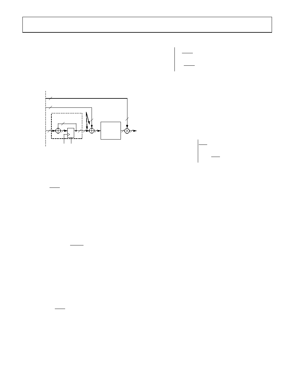
FUNCTIONAL BLOCK DETAIL
DDS CORE
The direct digital synthesizer (DDS) block generates a reference
signal (sine or cosine based on CFR1[16], the select DDS sine
output bit). The parameters of the reference signal (frequency,
phase, and amplitude) are applied to the DDS at its frequency,
phase offset, and amplitude control inputs, as shown in Figure 27.
06479-
010
DDS_CLK
32
19
FREQUENCY
CONTROL
ANGLE-TO-
AMPLITUDE
CONVERSION
(SINE OR
COSINE)
PHASE
OFFSET
CONTROL
TO DAC
(MSBs)
D Q
R
ACCUMULATOR
RESET
32
16
MSB ALIGNED
AMPLITUDE
CONTROL
14
DDS SIGNAL CONTROL PARAMETERS
16
14
19
32
14
32-BIT
ACCUMULATOR
Figure 27. DDS Block Diagram
The output frequency (fOUT) of the AD9910 is controlled by the
frequency tuning word (FTW) at the frequency control input to
the DDS. The relationship among fOUT, FTW, and fSYSCLK is given by
SYSCLK
OUT
f
FTW
f
=
32
2
(1)
where FTW is a 32-bit integer ranging in value from 0 to
2,147,483,647 (231 1), which represents the lower half of the
full 32-bit range. This range constitutes frequencies from dc to
Nyquist (that is, fSYSCLK).
The FTW required to generate a desired value of fOUT is found
by solving Equation 1 for FTW, as given in Equation 2.
=
SYSCLK
OUT
f
FTW
32
2
round
(2)
where the round(x) function rounds the argument (the value of
x) to the nearest integer. This is required because the FTW is
constrained to be an integer value. For example, for fOUT =
41 MHz and fSYSCLK = 122.88 MHz, then FTW = 1,433,053,867
(0x556AAAAB).
Programming an FTW greater than 231 produces an aliased
image that appears at a frequency given by
SYSCLK
OUT
f
FTW
f
=
32
2
1
(for FTW ≥ 231)
The relative phase of the DDS signal can be digitally controlled
by means of a 16-bit phase offset word (POW). The phase offset
is applied prior to the angle-to-amplitude conversion block
internal to the DDS core. The relative phase offset (Δθ) is given by
=
16
2
360
2
Δ
POW
π
θ
where the upper quantity is for the phase offset expressed as
radian units and the lower quantity as degrees. To find the POW
value necessary to develop an arbitrary Δθ, solve the previous
equation for POW and round the result (in a manner similar
to that described previously for finding an arbitrary FTW).
The relative amplitude of the DDS signal can be digitally scaled
(relative to full scale) by means of a 14-bit amplitude scale
factor (ASF). The amplitude scale value is applied at the output
of the angle-to-amplitude conversion block internal to the DDS
core. The amplitude scale is given by
=
14
2
log
20
2
ASF
Scale
Amplitude
(3)
where the upper quantity is amplitude expressed as a fraction of
full scale and the lower quantity is expressed in decibels relative
to full scale. To find the ASF value necessary for a particular
scale factor, solve Equation 3 for ASF and round the result (in
a manner similar to that described previously for finding an
arbitrary FTW).
When the AD9910 is programmed to modulate any of the DDS
signal control parameters, the maximum modulation sample
rate is fSYSCLK. This means that the modulation signal exhibits
images at multiples of fSYSCLK. The impact of these images
must be considered when using the device as a modulator.
14-BIT DAC OUTPUT
The AD9910 incorporates an integrated 14-bit, current output
DAC. The output current is delivered as a balanced signal using
two outputs. The use of balanced outputs reduces the potential
amount of common-mode noise present at the DAC output,
offering the advantage of an increased signal-to-noise ratio. An
external resistor (RSET) connected between the DAC_RSET pin
and AGND establishes the reference current. The full-scale
output current of the DAC (IOUT) is produced as a scaled version
of the reference current (see the Auxiliary DAC section). The
recommended value of RSET is 10 k.
Attention should be paid to the load termination to keep the
output voltage within the specified compliance range; voltages
developed beyond this range cause excessive distortion and can
damage the DAC output circuitry.
相关PDF资料 |
PDF描述 |
|---|---|
| MCF51EM128CLL | IC MCU 32BIT 128KB FLASH 100LQFP |
| AD9957BSVZ | IC DDS 1GSPS 14BIT IQ 100TQFP |
| AD9956YCPZ | IC SYNTHESIZER 1.8V 48LFCSP |
| S9S08DZ60F1MLH | MCU 60K FLASH MASK AUTO 64-LQFP |
| AD9952YSVZ | IC DDS 14BIT DAC 1.8V 48-TQFP |
相关代理商/技术参数 |
参数描述 |
|---|---|
| AD9910BSVZ | 制造商:Analog Devices 功能描述:IC DDS 1GHZ TQFP-100 制造商:Analog Devices 功能描述:IC, DDS, 1GHZ, TQFP-100 |
| AD9910BSVZ-REEL | 功能描述:IC DDS 1GSPS 14BIT PAR 100TQFP RoHS:是 类别:集成电路 (IC) >> 接口 - 直接数字合成 (DDS) 系列:- 产品变化通告:Product Discontinuance 27/Oct/2011 标准包装:2,500 系列:- 分辨率(位):10 b 主 fclk:25MHz 调节字宽(位):32 b 电源电压:2.97 V ~ 5.5 V 工作温度:-40°C ~ 85°C 安装类型:表面贴装 封装/外壳:16-TSSOP(0.173",4.40mm 宽) 供应商设备封装:16-TSSOP 包装:带卷 (TR) |
| AD9911 | 制造商:AD 制造商全称:Analog Devices 功能描述:500 MSPS Direct Digital Synthesizer with 10-Bit DAC |
| AD9911/PCB | 制造商:Analog Devices 功能描述:500 MSPS DIRECT DGTL SYNTHESIZER W/ 10-BIT DAC AD9911/PCB - Bulk |
| AD9911/PCBZ | 功能描述:BOARD EVAL FOR AD9911 RoHS:是 类别:编程器,开发系统 >> 评估演示板和套件 系列:AgileRF™ 标准包装:1 系列:PCI Express® (PCIe) 主要目的:接口,收发器,PCI Express 嵌入式:- 已用 IC / 零件:DS80PCI800 主要属性:- 次要属性:- 已供物品:板 |
发布紧急采购,3分钟左右您将得到回复。