- 您现在的位置:买卖IC网 > PDF目录10979 > AD9910BSVZ (Analog Devices Inc)IC DDS 1GSPS 14BIT PAR 100TQFP PDF资料下载
参数资料
| 型号: | AD9910BSVZ |
| 厂商: | Analog Devices Inc |
| 文件页数: | 3/64页 |
| 文件大小: | 0K |
| 描述: | IC DDS 1GSPS 14BIT PAR 100TQFP |
| 产品培训模块: | Direct Digital Synthesis Tutorial Series (1 of 7): Introduction Direct Digital Synthesizer Tutorial Series (7 of 7): DDS in Action Direct Digital Synthesis Tutorial Series (3 of 7): Angle to Amplitude Converter Direct Digital Synthesis Tutorial Series (6 of 7): SINC Envelope Correction Direct Digital Synthesis Tutorial Series (4 of 7): Digital-to-Analog Converter Direct Digital Synthesis Tutorial Series (2 of 7): The Accumulator |
| 设计资源: | Synchronizing Multiple AD9910 1 GSPS Direct Digital Synthesizers (CN0121) |
| 标准包装: | 1 |
| 分辨率(位): | 14 b |
| 主 fclk: | 1GHz |
| 调节字宽(位): | 32 b |
| 电源电压: | 1.8V, 3.3V |
| 工作温度: | -40°C ~ 85°C |
| 安装类型: | 表面贴装 |
| 封装/外壳: | 100-TQFP 裸露焊盘 |
| 供应商设备封装: | 100-TQFP-EP(14x14) |
| 包装: | 托盘 |
| 产品目录页面: | 552 (CN2011-ZH PDF) |
第1页第2页当前第3页第4页第5页第6页第7页第8页第9页第10页第11页第12页第13页第14页第15页第16页第17页第18页第19页第20页第21页第22页第23页第24页第25页第26页第27页第28页第29页第30页第31页第32页第33页第34页第35页第36页第37页第38页第39页第40页第41页第42页第43页第44页第45页第46页第47页第48页第49页第50页第51页第52页第53页第54页第55页第56页第57页第58页第59页第60页第61页第62页第63页第64页
Data Sheet
AD9910
Rev. D | Page 11 of 64
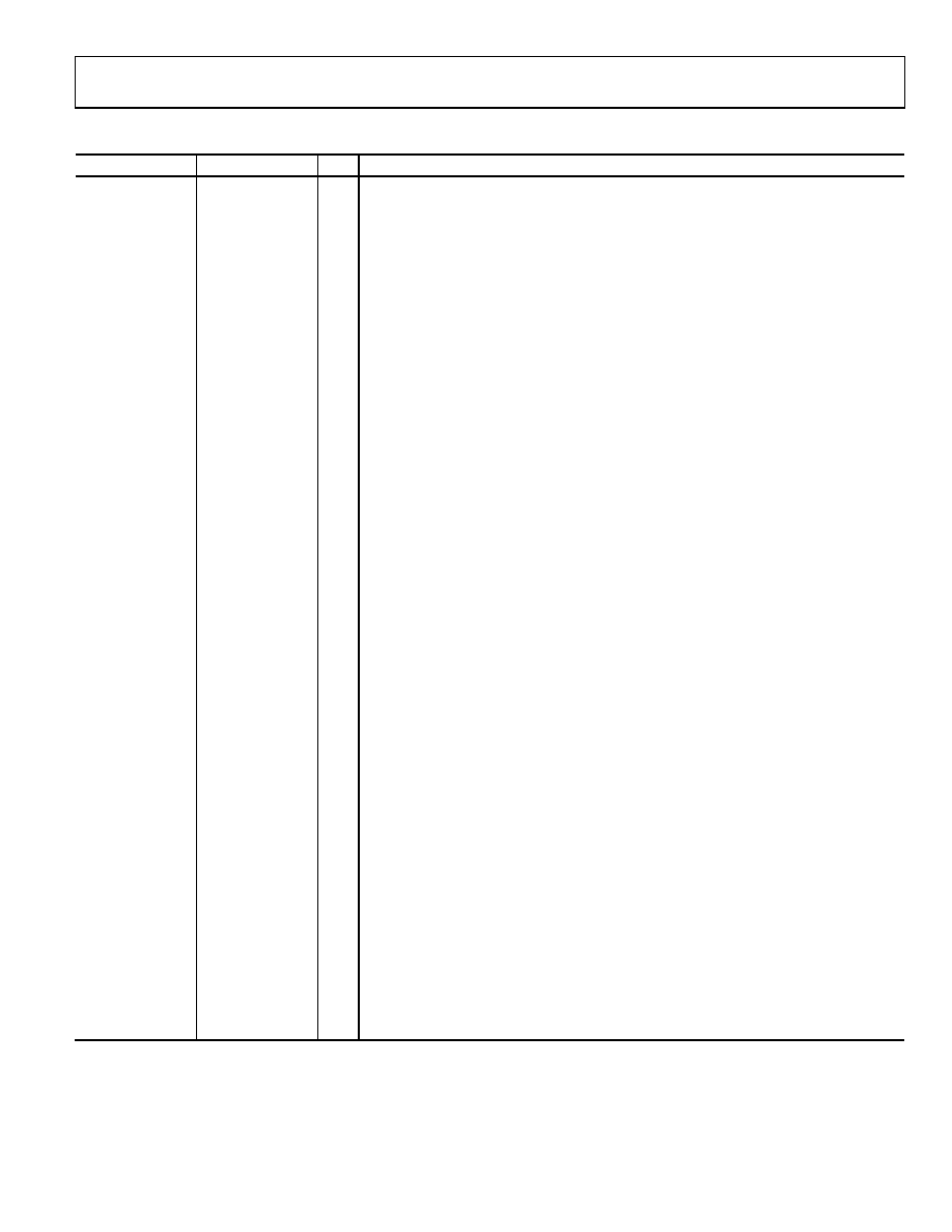
Table 3. Pin Function Descriptions
Pin No.
Mnemonic
I/O1
Description
1, 20, 72, 86, 87,
93, 97 to 100
NC
Not Connected. Allow device pins to float.
2
PLL_LOOP_FILTER
I
PLL Loop Filter Compensation Pin. See the External PLL Loop Filter Components section for
details.
3, 6, 89, 92
AVDD (1.8V)
I
Analog Core VDD, 1.8 V Analog Supplies.
74 to 77, 83
AVDD (3.3V)
I
Analog DAC VDD, 3.3 V Analog Supplies.
17, 23, 30, 47,
57, 64
DVDD (1.8V)
I
Digital Core VDD, 1.8 V Digital Supplies.
11, 15, 21, 28, 45,
56, 66
DVDD_I/O (3.3V)
I
Digital Input/Output VDD, 3.3 V Digital Supplies.
4, 5, 73, 78, 79, 82,
85, 88, 96
AGND
I
Analog Ground.
13, 16, 22, 29, 46,
51, 58, 65
DGND
I
Digital Ground.
7
SYNC_IN+
I
Synchronization Signal (LVDS), Digital Input (Rising Edge Active). The synchronization
signal from the external master to synchronize internal subclocks. See the Synchronization
of Multiple Devices section for details.
8
SYNC_IN
I
Synchronization Signal (LVDS), Digital Input. The synchronization signal from the external
master to synchronize internal subclocks. See the Synchronization of Multiple Devices
section for details.
9
SYNC_OUT+
O
Synchronization Signal (LVDS), Digital Output (Rising Edge Active). The synchronization
signal from the internal device subclocks to synchronize external slave devices. See the
Synchronization of Multiple Devices section for details.
10
SYNC_OUT
O
Synchronization Signal (LVDS), Digital Output. The synchronization signal from the internal
device subclocks to synchronize external slave devices. See the Synchronization of Multiple
Devices section for details.
12
SYNC_SMP_ERR
O
Synchronization Sample Error, Digital Output (Active High). Sync sample error: a high on
this pin indicates that the AD9910 did not receive a valid sync signal on SYNC_IN+/SYNC_IN.
14
MASTER_RESET
I
Master Reset, Digital Input (Active High). Master reset: clears all memory elements and sets
registers to default values.
18
EXT_PWR_DWN
I
External Power-Down, Digital Input (Active High). A high level on this pin initiates the
currently programmed power-down mode. See the Power-Down Control section for
further details. If unused, connect to ground.
19
PLL_LOCK
O
Clock Multiplier PLL Lock, Digital Output (Active High). A high on this pin indicates that the
Clock Multiplier PLL has acquired lock to the reference clock input.
24
RAM_SWP_OVR
O
RAM Sweep Over, Digital Output (Active High). A high on this pin indicates that the RAM
sweep profile has completed.
25 to 27, 31 to 39,
42 to 44, 48
D[15:0]
I
Parallel Input Bus (Active High).
49, 50
F[1:0]
I
Modulation Format Pins. Digital input to determine the modulation format.
40
PDCLK
O
Parallel Data Clock. This is the digital output (clock). The parallel data clock provides a
timing signal for aligning data at the parallel inputs.
41
TxENABLE
I
Transmit Enable. Digital input (active high). In burst mode communications, a high on this
pin indicates new data for transmission. In continuous mode, this pin remains high.
52 to 54
PROFILE[2:0]
I
Profile Select Pins. Digital inputs (active high). Use these pins to select one of eight
phase/frequency profiles for the DDS. Changing the state of one of these pins transfers the
current contents of all I/O buffers to the corresponding registers. State changes should be
set up on the SYNC_CLK pin.
55
SYNC_CLK
O
Output Clock Divided-By-Four. A digital output (clock). Many of the digital inputs on the
chip, such as I/O_UPDATE and PROFILE[2:0], need to be set up on the rising edge of this signal.
相关PDF资料 |
PDF描述 |
|---|---|
| MCF51EM128CLL | IC MCU 32BIT 128KB FLASH 100LQFP |
| AD9957BSVZ | IC DDS 1GSPS 14BIT IQ 100TQFP |
| AD9956YCPZ | IC SYNTHESIZER 1.8V 48LFCSP |
| S9S08DZ60F1MLH | MCU 60K FLASH MASK AUTO 64-LQFP |
| AD9952YSVZ | IC DDS 14BIT DAC 1.8V 48-TQFP |
相关代理商/技术参数 |
参数描述 |
|---|---|
| AD9910BSVZ | 制造商:Analog Devices 功能描述:IC DDS 1GHZ TQFP-100 制造商:Analog Devices 功能描述:IC, DDS, 1GHZ, TQFP-100 |
| AD9910BSVZ-REEL | 功能描述:IC DDS 1GSPS 14BIT PAR 100TQFP RoHS:是 类别:集成电路 (IC) >> 接口 - 直接数字合成 (DDS) 系列:- 产品变化通告:Product Discontinuance 27/Oct/2011 标准包装:2,500 系列:- 分辨率(位):10 b 主 fclk:25MHz 调节字宽(位):32 b 电源电压:2.97 V ~ 5.5 V 工作温度:-40°C ~ 85°C 安装类型:表面贴装 封装/外壳:16-TSSOP(0.173",4.40mm 宽) 供应商设备封装:16-TSSOP 包装:带卷 (TR) |
| AD9911 | 制造商:AD 制造商全称:Analog Devices 功能描述:500 MSPS Direct Digital Synthesizer with 10-Bit DAC |
| AD9911/PCB | 制造商:Analog Devices 功能描述:500 MSPS DIRECT DGTL SYNTHESIZER W/ 10-BIT DAC AD9911/PCB - Bulk |
| AD9911/PCBZ | 功能描述:BOARD EVAL FOR AD9911 RoHS:是 类别:编程器,开发系统 >> 评估演示板和套件 系列:AgileRF™ 标准包装:1 系列:PCI Express® (PCIe) 主要目的:接口,收发器,PCI Express 嵌入式:- 已用 IC / 零件:DS80PCI800 主要属性:- 次要属性:- 已供物品:板 |
发布紧急采购,3分钟左右您将得到回复。