- 您现在的位置:买卖IC网 > PDF目录10979 > AD9910BSVZ (Analog Devices Inc)IC DDS 1GSPS 14BIT PAR 100TQFP PDF资料下载
参数资料
| 型号: | AD9910BSVZ |
| 厂商: | Analog Devices Inc |
| 文件页数: | 4/64页 |
| 文件大小: | 0K |
| 描述: | IC DDS 1GSPS 14BIT PAR 100TQFP |
| 产品培训模块: | Direct Digital Synthesis Tutorial Series (1 of 7): Introduction Direct Digital Synthesizer Tutorial Series (7 of 7): DDS in Action Direct Digital Synthesis Tutorial Series (3 of 7): Angle to Amplitude Converter Direct Digital Synthesis Tutorial Series (6 of 7): SINC Envelope Correction Direct Digital Synthesis Tutorial Series (4 of 7): Digital-to-Analog Converter Direct Digital Synthesis Tutorial Series (2 of 7): The Accumulator |
| 设计资源: | Synchronizing Multiple AD9910 1 GSPS Direct Digital Synthesizers (CN0121) |
| 标准包装: | 1 |
| 分辨率(位): | 14 b |
| 主 fclk: | 1GHz |
| 调节字宽(位): | 32 b |
| 电源电压: | 1.8V, 3.3V |
| 工作温度: | -40°C ~ 85°C |
| 安装类型: | 表面贴装 |
| 封装/外壳: | 100-TQFP 裸露焊盘 |
| 供应商设备封装: | 100-TQFP-EP(14x14) |
| 包装: | 托盘 |
| 产品目录页面: | 552 (CN2011-ZH PDF) |
第1页第2页第3页当前第4页第5页第6页第7页第8页第9页第10页第11页第12页第13页第14页第15页第16页第17页第18页第19页第20页第21页第22页第23页第24页第25页第26页第27页第28页第29页第30页第31页第32页第33页第34页第35页第36页第37页第38页第39页第40页第41页第42页第43页第44页第45页第46页第47页第48页第49页第50页第51页第52页第53页第54页第55页第56页第57页第58页第59页第60页第61页第62页第63页第64页
AD9910
Data Sheet
Rev. D | Page 12 of 64
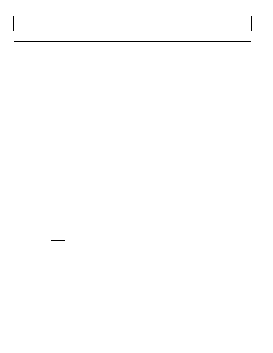
Pin No.
Mnemonic
I/O1
Description
59
I/O_UPDATE
I/O
Input/Output Update. Digital input (active high). A high on this pin transfers the contents
of the I/O buffers to the corresponding internal registers.
60
OSK
I
Output Shift Keying. Digital input (active high). When the OSK features are placed in either
manual or automatic mode, this pin controls the OSK function. In manual mode, it toggles
the multiplier between 0 (low) and the programmed amplitude scale factor (high). In
automatic mode, a low sweeps the amplitude down to zero, a high sweeps the amplitude
up to the amplitude scale factor.
61
DROVER
O
Digital Ramp Over. Digital output (active high). This pin switches to Logic 1 whenever the
digital ramp generator reaches its programmed upper or lower limit.
62
DRCTL
I
Digital Ramp Control. Digital input (active high). This pin controls the slope polarity of the
digital ramp generator. See the Digital Ramp Generator (DRG) section for more details. If
not using the digital ramp generator, connect this pin to Logic 0.
63
DRHOLD
I
Digital Ramp Hold. Digital input (active high). This pin stalls the digital ramp generator in
its present state. See the Digital Ramp Generator (DRG) section for more details. If not
using a digital ramp generator, connect this pin to Logic 0.
67
SDIO
I/O
Serial Data Input/Output. Digital input/output (active high). This pin can be either unidirec-
tional or bidirectional (default), depending on the configuration settings. In bidirectional serial
port mode, this pin acts as the serial data input and output. In unidirectional mode, it is an
input only.
68
SDO
O
Serial Data Output. Digital output (active high). This pin is only active in unidirectional
serial data mode. In this mode, it functions as the output. In bidirectional mode, this pin is
not operational and should be left floating.
69
SCLK
I
Serial Data Clock. Digital clock (rising edge on write, falling edge on read). This pin provides
the serial data clock for the control data path. Write operations to the AD9910 use the
rising edge. Readback operations from the AD9910 use the falling edge.
70
CS
I
Chip Select. Digital input (active low). This pin allows the AD9910 to operate on a common
serial bus for the control data path. Bringing this pin low enables the AD9910 to detect
serial clock rising/falling edges. Bringing this pin high causes the AD9910 to ignore input
on the serial data pins.
71
I/O_RESET
I
Input/Output Reset. Digital input (active high). This pin can be used when a serial I/O
communication cycle fails (see the I/O_RESET—Input/Output Reset section for details).
When not used, connect this pin to ground.
80
IOUT
O
Open-Drain DAC Complementary Output Source. Analog output (current mode). Connect
through a 50 resistor to AGND.
81
IOUT
O
Open-Drain DAC Output Source. Analog output (current mode). Connect through a 50
resistor to AGND.
84
DAC_RSET
O
Analog Reference Pin. This pin programs the DAC output full-scale reference current.
Attach a 10 k resistor to AGND.
90
REF_CLK
I
Reference Clock Input. Analog input. When the internal oscillator is engaged, this pin can
be driven by either an external oscillator or connected to a crystal. See the REF_CLK/ Overview
section for more details.
91
REF_CLK
I
Reference Clock Input. Analog input. See the REF_CLK/ Overview section for more details.
94
REFCLK_OUT
O
Crystal Output. Analog output. See the REF_CLK/ Overview section for more details.
95
XTAL_SEL
I
Crystal Select (1.8 V Logic). Analog input (active high). Driving the XTAL_SEL pin high,
the AVDD (1.8V) pin enables the internal oscillator to be used with a crystal resonator.
If unused, connect it to AGND.
EPAD
Exposed Paddle
(EPAD)
The EPAD should be soldered to ground.
1 I = input, O = output.
相关PDF资料 |
PDF描述 |
|---|---|
| MCF51EM128CLL | IC MCU 32BIT 128KB FLASH 100LQFP |
| AD9957BSVZ | IC DDS 1GSPS 14BIT IQ 100TQFP |
| AD9956YCPZ | IC SYNTHESIZER 1.8V 48LFCSP |
| S9S08DZ60F1MLH | MCU 60K FLASH MASK AUTO 64-LQFP |
| AD9952YSVZ | IC DDS 14BIT DAC 1.8V 48-TQFP |
相关代理商/技术参数 |
参数描述 |
|---|---|
| AD9910BSVZ | 制造商:Analog Devices 功能描述:IC DDS 1GHZ TQFP-100 制造商:Analog Devices 功能描述:IC, DDS, 1GHZ, TQFP-100 |
| AD9910BSVZ-REEL | 功能描述:IC DDS 1GSPS 14BIT PAR 100TQFP RoHS:是 类别:集成电路 (IC) >> 接口 - 直接数字合成 (DDS) 系列:- 产品变化通告:Product Discontinuance 27/Oct/2011 标准包装:2,500 系列:- 分辨率(位):10 b 主 fclk:25MHz 调节字宽(位):32 b 电源电压:2.97 V ~ 5.5 V 工作温度:-40°C ~ 85°C 安装类型:表面贴装 封装/外壳:16-TSSOP(0.173",4.40mm 宽) 供应商设备封装:16-TSSOP 包装:带卷 (TR) |
| AD9911 | 制造商:AD 制造商全称:Analog Devices 功能描述:500 MSPS Direct Digital Synthesizer with 10-Bit DAC |
| AD9911/PCB | 制造商:Analog Devices 功能描述:500 MSPS DIRECT DGTL SYNTHESIZER W/ 10-BIT DAC AD9911/PCB - Bulk |
| AD9911/PCBZ | 功能描述:BOARD EVAL FOR AD9911 RoHS:是 类别:编程器,开发系统 >> 评估演示板和套件 系列:AgileRF™ 标准包装:1 系列:PCI Express® (PCIe) 主要目的:接口,收发器,PCI Express 嵌入式:- 已用 IC / 零件:DS80PCI800 主要属性:- 次要属性:- 已供物品:板 |
发布紧急采购,3分钟左右您将得到回复。