参数资料
| 型号: | AD9948KCPZ |
| 厂商: | Analog Devices Inc |
| 文件页数: | 11/28页 |
| 文件大小: | 0K |
| 描述: | IC CCD SIGNAL PROCESSOR 40-LFCSP |
| 标准包装: | 1 |
| 类型: | CCD 信号处理器,10 位 |
| 输入类型: | 逻辑 |
| 输出类型: | 逻辑 |
| 接口: | 3 线串口 |
| 安装类型: | 表面贴装 |
| 封装/外壳: | 40-VFQFN 裸露焊盘,CSP |
| 供应商设备封装: | 40-LFCSP |
| 包装: | 托盘 |
第1页第2页第3页第4页第5页第6页第7页第8页第9页第10页当前第11页第12页第13页第14页第15页第16页第17页第18页第19页第20页第21页第22页第23页第24页第25页第26页第27页第28页
REV. 0
AD9948
–19–
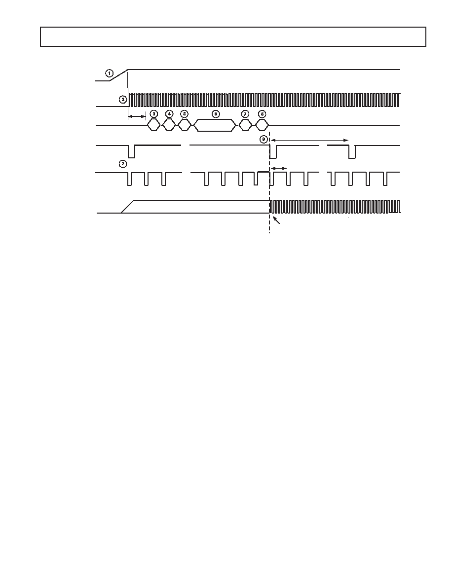
POWER-UP PROCEDURE
VDD
(INPUT)
SERIAL
WRITES
VD
(OUTPUT)
1 H
ODD FIELD
EVEN FIELD
...
DIGITAL
OUTPUTS
CLOCKS ACTIVE WHEN OUT_CONTROL REGISTER IS
UPDATED AT VD/HD EDGE
H1/H3, RG
H2/H4
tPWR
CLI
(INPUT)
HD
(OUTPUT)
1V
...
Figure 14. Recommended Power-Up Sequence
Recommended Power-Up Sequence
When the AD9948 is powered up, the following sequence is
recommended (refer to Figure 14 for each step):
1. Turn on the power supplies for the AD9948.
2. Apply the master clock input, CLI, VD, and HD.
3. Although the AD9948 contains an on-chip power-on reset, a
software reset of the internal registers is recommended. Write
a 1 to the SW_RST register (Address x010), which will reset
all the internal registers to their default values. This bit is
self-clearing and will automatically be reset back to 0.
4. The Precision Timing core must be reset by writing a 0 to the
TGCORE_RSTB register (Address x012) followed by writing
a l to the TGCORE_RSTB register. This will start the internal
timing core operation.
5. Write a 1 to the PREVENTUPDATE register (Address x014).
This will prevent the updating of the serial register data.
6. Write to the desired registers to configure high speed timing
and horizontal timing.
7. Write a 1 to the OUT_CONTROL register (Address x011).
This will allow the outputs to become active after the next
VD/HD rising edge.
8. Write a 0 to the PREVENTUPDATE register (Address x014).
This will allow the serial information to be updated at next
VD/HD falling edge.
The next VD/HD falling edge allows register updates to occur,
including OUT_CONTROL, which enables all clock outputs.
相关PDF资料 |
PDF描述 |
|---|---|
| AD9949KCPZ | IC CCD SIGNAL PROCESSOR 40-LFCSP |
| AD9951YSVZ | IC DDS DAC 14BIT 1.8V 48-TQFP |
| AD9952YSVZ-REEL7 | IC DDS DAC 14BIT 1.8V 48TQFP |
| AD9953YSVZ-REEL7 | IC DDS DAC 14BIT 1.8V 48TQFP |
| AD9954YSVZ-REEL7 | IC DDS DAC 14BIT 1.8V 48TQFP |
相关代理商/技术参数 |
参数描述 |
|---|---|
| AD9948KCPZRL | 功能描述:IC CCD SIGNAL PROCESSOR 40-LFCSP RoHS:是 类别:集成电路 (IC) >> 接口 - 传感器和探测器接口 系列:- 其它有关文件:Automotive Product Guide 产品培训模块:Lead (SnPb) Finish for COTS Obsolescence Mitigation Program 标准包装:74 系列:- 类型:触控式传感器 输入类型:数字 输出类型:数字 接口:JTAG,串行 电流 - 电源:100µA 安装类型:表面贴装 封装/外壳:20-TSSOP(0.173",4.40mm 宽) 供应商设备封装:20-TSSOP 包装:管件 |
| AD9949 | 制造商:AD 制造商全称:Analog Devices 功能描述:12-Bit CCD Signal Processor with Precision Timing Core |
| AD9949AKCPZ | 功能描述:IC CCD SIGNAL PROCESSOR 40-LFCSP RoHS:是 类别:集成电路 (IC) >> 接口 - 传感器和探测器接口 系列:- 其它有关文件:Automotive Product Guide 产品培训模块:Lead (SnPb) Finish for COTS Obsolescence Mitigation Program 标准包装:74 系列:- 类型:触控式传感器 输入类型:数字 输出类型:数字 接口:JTAG,串行 电流 - 电源:100µA 安装类型:表面贴装 封装/外壳:20-TSSOP(0.173",4.40mm 宽) 供应商设备封装:20-TSSOP 包装:管件 |
| AD9949AKCPZRL | 功能描述:IC CCD SIGNAL PROCESSOR 40-LFCSP RoHS:是 类别:集成电路 (IC) >> 接口 - 传感器和探测器接口 系列:- 其它有关文件:Automotive Product Guide 产品培训模块:Lead (SnPb) Finish for COTS Obsolescence Mitigation Program 标准包装:74 系列:- 类型:触控式传感器 输入类型:数字 输出类型:数字 接口:JTAG,串行 电流 - 电源:100µA 安装类型:表面贴装 封装/外壳:20-TSSOP(0.173",4.40mm 宽) 供应商设备封装:20-TSSOP 包装:管件 |
| AD9949BCBZRL | 制造商:Analog Devices 功能描述: |
发布紧急采购,3分钟左右您将得到回复。