- 您现在的位置:买卖IC网 > PDF目录10978 > AD9954YSVZ (Analog Devices Inc)IC DDS DAC 14BIT 1.8V 48-TQFP PDF资料下载
参数资料
| 型号: | AD9954YSVZ |
| 厂商: | Analog Devices Inc |
| 文件页数: | 14/40页 |
| 文件大小: | 0K |
| 描述: | IC DDS DAC 14BIT 1.8V 48-TQFP |
| 产品培训模块: | Direct Digital Synthesis Tutorial Series (1 of 7): Introduction Direct Digital Synthesizer Tutorial Series (7 of 7): DDS in Action Direct Digital Synthesis Tutorial Series (3 of 7): Angle to Amplitude Converter Direct Digital Synthesis Tutorial Series (6 of 7): SINC Envelope Correction Direct Digital Synthesis Tutorial Series (4 of 7): Digital-to-Analog Converter Direct Digital Synthesis Tutorial Series (2 of 7): The Accumulator |
| 标准包装: | 1 |
| 分辨率(位): | 14 b |
| 主 fclk: | 400MHz |
| 调节字宽(位): | 32 b |
| 电源电压: | 1.71 V ~ 1.96 V |
| 工作温度: | -40°C ~ 105°C |
| 安装类型: | 表面贴装 |
| 封装/外壳: | 48-TQFP 裸露焊盘 |
| 供应商设备封装: | 48-TQFP 裸露焊盘(7x7) |
| 包装: | 托盘 |
| 产品目录页面: | 552 (CN2011-ZH PDF) |
| 配用: | AD9954/PCBZ-ND - BOARD EVAL FOR 9954 |
第1页第2页第3页第4页第5页第6页第7页第8页第9页第10页第11页第12页第13页当前第14页第15页第16页第17页第18页第19页第20页第21页第22页第23页第24页第25页第26页第27页第28页第29页第30页第31页第32页第33页第34页第35页第36页第37页第38页第39页第40页
AD9954
Rev. B | Page 21 of 40
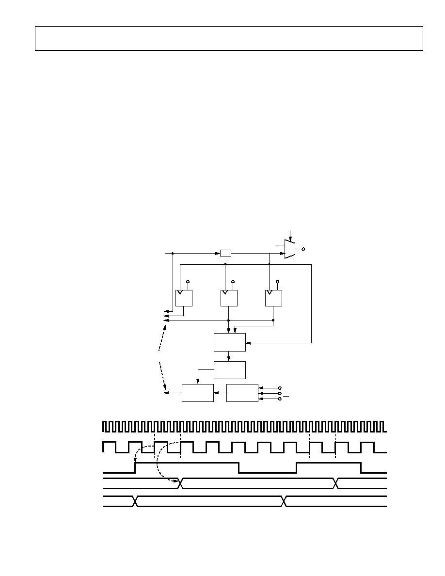
SYNCHRONIZATION—REGISTER UPDATES (I/O
UPDATE)
Functionality of the SYNC_CLK and I/O UPDATE
Data into the AD9954 is synchronous to the SYNC_CLK
signal (supplied externally to the user on the SYNC_CLK pin).
The I/O UPDATE pin is sampled on the rising edge of the
SYNC_CLK.
Internally, SYSCLK is fed to a divide-by-four frequency divider
to produce the SYNC_CLK signal. The SYNC_CLK signal is
made available to the system on the SYNC_CLK pin. This
enables synchronization of external hardware with the device’s
internal clocks. This is accomplished by providing the SYNC_CLK
signal as an output that external hardware can then use to
synchronize against.
The I/O update signal coupled with SYNC_CLK is used to
transfer internal buffer contents into the control registers. The
combination of the SYNC_CLK pin and the I/O UPDATE pin
provides the user with constant latency relative to SYSCLK and
ensures phase continuity of the analog output signal when a
new tuning word or phase offset value is asserted.
Figure 23 and Figure 24 demonstrate an I/O update timing
cycle and synchronization.
Synchronization logic notes include the following:
The I/O update signal is edge detected to generate a single-
cycle clock signal that drives the register bank flops. The I/O
update signal has no constraints on duty cycle. The minimum
low time on I/O update is one SYNC_CLK clock cycle.
The I/O UPDATE pin is set up and held around the rising
edge of SYNC_CLK. Setup and hold time specifications can
be found in Table 2.
03
37
4-
0
6
SYSCLK
SDIO
SYNC_CLK
DISABLE
10
0
SCLK
TO CORE LOGIC
CS
OSK
D
Q
PS<1:0>
D
Q
I/O UPDATE
D
Q
÷4
SYNC_CLK
GATING
EDGE
DETECTION
LOGIC
REGISTER
MEMORY
I/O BUFFER
LATCHES
Figure 23. I/O Synchronization Block Diagram
SYNC_CLK
SYSCLK
AB
DATA IN
REGISTERS
DATA IN
I/O BUFFERS
I/O UPDATE
THE DEVICE REGISTERS AN I/O UPDATE AT POINT A. THE DATA IS TRANSFERRED FROM
THE ASYNCHRONOUSLY LOADED I/O BUFFERS AT POINT B.
0
33
74
-0
07
N – 1
N
N + 1
N
N + 1
N + 2
Figure 24. I/O Synchronization Timing Diagram
相关PDF资料 |
PDF描述 |
|---|---|
| AD9911BCPZ | IC DDS 500MSPS DAC 10BIT 56LFCSP |
| VE-B11-IY-F4 | CONVERTER MOD DC/DC 12V 50W |
| VE-B11-IY-F1 | CONVERTER MOD DC/DC 12V 50W |
| VE-2WZ-IY-F4 | CONVERTER MOD DC/DC 2V 20W |
| VE-2WZ-IY-F1 | CONVERTER MOD DC/DC 2V 20W |
相关代理商/技术参数 |
参数描述 |
|---|---|
| AD9954YSVZ | 制造商:Analog Devices 功能描述:IC DDS 400MSPS SMD 9954 TQFP48 |
| AD9954YSVZ1 | 制造商:AD 制造商全称:Analog Devices 功能描述:400 MSPS, 14-Bit, 1.8 V CMOS, Direct Digital Synthesizer |
| AD9954YSVZ-REEL7 | 功能描述:IC DDS DAC 14BIT 1.8V 48TQFP RoHS:是 类别:集成电路 (IC) >> 接口 - 直接数字合成 (DDS) 系列:- 产品变化通告:Product Discontinuance 27/Oct/2011 标准包装:2,500 系列:- 分辨率(位):10 b 主 fclk:25MHz 调节字宽(位):32 b 电源电压:2.97 V ~ 5.5 V 工作温度:-40°C ~ 85°C 安装类型:表面贴装 封装/外壳:16-TSSOP(0.173",4.40mm 宽) 供应商设备封装:16-TSSOP 包装:带卷 (TR) |
| AD9954YSVZ-REEL71 | 制造商:AD 制造商全称:Analog Devices 功能描述:400 MSPS, 14-Bit, 1.8 V CMOS, Direct Digital Synthesizer |
| AD9955KS6 | 制造商:AD 功能描述:* |
发布紧急采购,3分钟左右您将得到回复。