- 您现在的位置:买卖IC网 > PDF目录2139 > ADA4940-1ARZ-R7 (Analog Devices Inc)IC DIFF ADC DVR 18BIT LN 8SOIC PDF资料下载
参数资料
| 型号: | ADA4940-1ARZ-R7 |
| 厂商: | Analog Devices Inc |
| 文件页数: | 16/33页 |
| 文件大小: | 0K |
| 描述: | IC DIFF ADC DVR 18BIT LN 8SOIC |
| 标准包装: | 1,000 |
| 放大器类型: | 差分 |
| 电路数: | 1 |
| 输出类型: | 差分 |
| 转换速率: | 95 V/µs |
| -3db带宽: | 260MHz |
| 电流 - 输入偏压: | 1.1µA |
| 电压 - 输入偏移: | 60µV |
| 电流 - 电源: | 1.25mA |
| 电流 - 输出 / 通道: | 46mA |
| 电压 - 电源,单路/双路(±): | 3 V ~ 6 V |
| 工作温度: | -40°C ~ 125°C |
| 安装类型: | 表面贴装 |
| 封装/外壳: | 8-SOIC(0.154",3.90mm 宽) |
| 供应商设备封装: | 8-SO |
| 包装: | 带卷 (TR) |
第1页第2页第3页第4页第5页第6页第7页第8页第9页第10页第11页第12页第13页第14页第15页当前第16页第17页第18页第19页第20页第21页第22页第23页第24页第25页第26页第27页第28页第29页第30页第31页第32页第33页
ADA4940-1/ADA4940-2
Data Sheet
Rev. C | Page 22 of 32
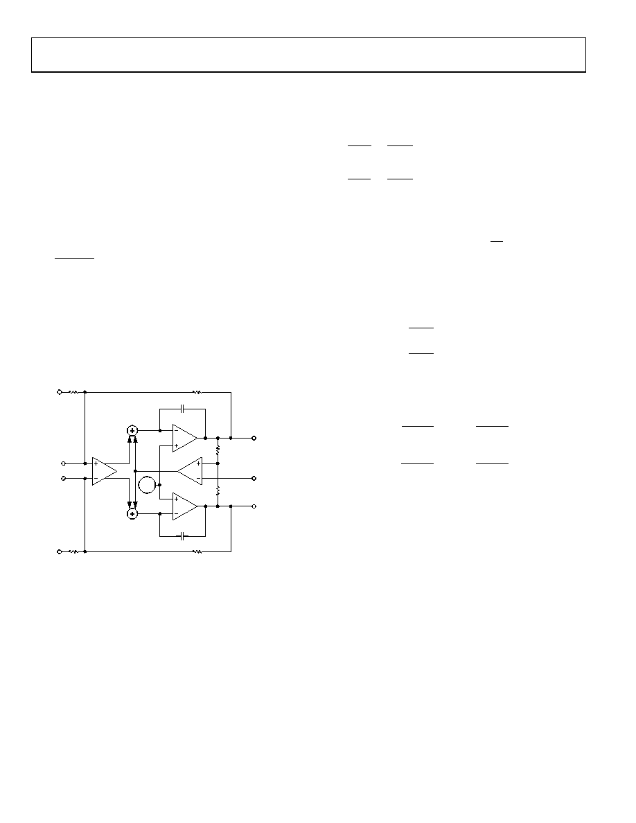
THEORY OF OPERATION
The ADA4940-1/ADA4940-2 are high speed, low power
differential amplifiers fabricated on Analog Devices advanced
dielectrically isolated SiGe bipolar process. They provide two
closely balanced differential outputs in response to either
differential or single-ended input signals. An external feedback
network that is similar to a voltage feedback operational
amplifier sets the differential gain. The output common-mode
voltage is independent of the input common-mode voltage and
is set by an external voltage at the VOCM terminal. The PNP
input stage allows input common-mode voltages between the
negative supply and 1.2 V below the positive supply. A rail-to-
rail output stage supplies a wide output voltage range.
The DISABLE pin can be used to reduce the supply current of
the amplifier to 13.5 A.
The differential feedback loop consists of the differential trans-
conductance GDIFF working through the GO output buffers and
the RF/RG feedback networks. The common-mode feedback
loop is set up with a voltage divider across the two differential
outputs to create an output voltage midpoint and a common-
mode transconductance, GCM.
08452-
058
GO
CC
RF
RG
GCM
GDIFF
GO
RG
VREF
–OUT
+OUT
RF
+DIN
–DIN
+IN
–IN
VOCM
Figure 62. ADA4940-1/ADA4940-2 Architectural Block
The differential feedback loop forces the voltages at +IN and IN
to equal each other. This fact sets the following relationships:
F
OUT
G
IN
R
V
R
D
=
+
F
OUT
G
IN
R
V
R
D
+
=
Subtracting the previous equations gives the relationship that
shows RF and RG setting the differential gain.
(V+OUT VOUT) = (+DIN – (DIN)) ×
G
F
R
The common-mode feedback loop drives the output common-
mode voltage that is sampled at the midpoint of the output
voltage divider to equal the voltage at VOCM. This results in the
following relationships:
V+OUT = VOCM +
2
dm
OUT,
V
VOUT = VOCM
2
dm
OUT,
V
Note that the differential amplifier’s summing junction input
voltages, +IN and IN, are set by both the output voltages and
the input voltages.
+
+
=
+
G
F
G
OUT
G
F
IN
R
V
R
D
V
+
+
=
+
G
F
G
OUT
G
F
IN
R
V
R
D
V
相关PDF资料 |
PDF描述 |
|---|---|
| ADA4950-1YCPZ-RL | IC AMP DIFF LP 114MA 16LFCSP |
| ADEL2020ARZ-20-RL | IC OPAMP CF LN LP 60MA 20SOIC |
| ADL5561ACPZ-R7 | IC AMP DIFF RF/IF 2.9GHZ 16LFCSP |
| ADL5562ACPZ-R7 | IC AMP DIFF RF/IF 3.3GHZ 16LFCSP |
| ADL5565ACPZ-R7 | IC AMP DIFF 6GHZ 16LFCSP |
相关代理商/技术参数 |
参数描述 |
|---|---|
| ADA4940-1ARZ-RL | 功能描述:IC DIFF ADC DVR 18BIT LN 8SOIC RoHS:是 类别:集成电路 (IC) >> Linear - Amplifiers - Instrumentation 系列:- 标准包装:50 系列:- 放大器类型:通用 电路数:2 输出类型:满摆幅 转换速率:1.8 V/µs 增益带宽积:6.5MHz -3db带宽:4.5MHz 电流 - 输入偏压:5nA 电压 - 输入偏移:100µV 电流 - 电源:65µA 电流 - 输出 / 通道:35mA 电压 - 电源,单路/双路(±):1.8 V ~ 5.25 V,±0.9 V ~ 2.625 V 工作温度:-40°C ~ 85°C 安装类型:表面贴装 封装/外壳:10-TFSOP,10-MSOP(0.118",3.00mm 宽) 供应商设备封装:10-MSOP 包装:管件 |
| ADA4940-1XCPZ-R7 | 制造商:Analog Devices 功能描述: |
| ADA4940-2 | 制造商:AD 制造商全称:Analog Devices 功能描述:Ultralow Power, Low Distortion |
| ADA4940-2ACP-EBZ | 制造商:Analog Devices 功能描述:EVAL BOARD DUAL DIFFERENTIAL 制造商:Analog Devices 功能描述:ADA4940-2, DIFF AMP, EVAL BOARD |
| ADA4940-2ACPZ-R2 | 制造商:Analog Devices 功能描述:SUB 10M W ADC DRIVER FOR PULSAR FAMILY - Tape and Reel |
发布紧急采购,3分钟左右您将得到回复。