- 您现在的位置:买卖IC网 > PDF目录2139 > ADA4940-1ARZ-R7 (Analog Devices Inc)IC DIFF ADC DVR 18BIT LN 8SOIC PDF资料下载
参数资料
| 型号: | ADA4940-1ARZ-R7 |
| 厂商: | Analog Devices Inc |
| 文件页数: | 33/33页 |
| 文件大小: | 0K |
| 描述: | IC DIFF ADC DVR 18BIT LN 8SOIC |
| 标准包装: | 1,000 |
| 放大器类型: | 差分 |
| 电路数: | 1 |
| 输出类型: | 差分 |
| 转换速率: | 95 V/µs |
| -3db带宽: | 260MHz |
| 电流 - 输入偏压: | 1.1µA |
| 电压 - 输入偏移: | 60µV |
| 电流 - 电源: | 1.25mA |
| 电流 - 输出 / 通道: | 46mA |
| 电压 - 电源,单路/双路(±): | 3 V ~ 6 V |
| 工作温度: | -40°C ~ 125°C |
| 安装类型: | 表面贴装 |
| 封装/外壳: | 8-SOIC(0.154",3.90mm 宽) |
| 供应商设备封装: | 8-SO |
| 包装: | 带卷 (TR) |
第1页第2页第3页第4页第5页第6页第7页第8页第9页第10页第11页第12页第13页第14页第15页第16页第17页第18页第19页第20页第21页第22页第23页第24页第25页第26页第27页第28页第29页第30页第31页第32页当前第33页
ADA4940-1/ADA4940-2
Data Sheet
Rev. C | Page 8 of 32
ABSOLUTE MAXIMUM RATINGS
Table 9.
Parameter
Rating
Supply Voltage
8 V
VOCM
±VS
Differential Input Voltage
1.2 V
Operating Temperature Range
40°C to +125°C
Storage Temperature Range
65°C to +150°C
Lead Temperature (Soldering, 10 sec)
300°C
Junction Temperature
150°C
ESD
Field Induced Charged Device Model (FICDM)
1250 V
Human Body Model (HBM)
2000 V
Stresses above those listed under Absolute Maximum Ratings
may cause permanent damage to the device. This is a stress
rating only; functional operation of the device at these or any
other conditions above those indicated in the operational
section of this specification is not implied. Exposure to absolute
maximum rating conditions for extended periods may affect
device reliability.
THERMAL RESISTANCE
θJA is specified for the worst-case conditions, that is, θJA is
specified for the device soldered on a circuit board in still air.
Table 10.
Package Type
θJA
Unit
8-Lead SOIC (Single)/4-Layer Board
158
°C/W
16-Lead LFCSP (Single)/4-Layer Board
91.3
°C/W
24-Lead LFCSP (Dual)/4-Layer Board
65.1
°C/W
MAXIMUM POWER DISSIPATION
The maximum safe power dissipation in the ADA4940-1/
ADA4940-2 packages is limited by the associated rise in
junction temperature (TJ) on the die. At approximately 150°C,
which is the glass transition temperature, the plastic changes its
properties. Even temporarily exceeding this temperature limit
can change the stresses that the package exerts on the die,
permanently shifting the parametric performance of the
ADA4940-1/ADA4940-2. Exceeding a junction temperature
of 150°C for an extended period can result in changes in the
silicon devices, potentially causing failure.
The power dissipated in the package (PD) is the sum of the
quiescent power dissipation and the power dissipated in the
package due to the load drive for all outputs. The quiescent
power dissipation is the voltage between the supply pins (±VS)
times the quiescent current (IS). The load current consists of the
differential and common-mode currents flowing to the load, as
well as currents flowing through the external feedback networks
and internal common-mode feedback loop. The internal
resistor tap used in the common-mode feedback loop places a
negligible differential load on the output. RMS voltages and
currents should be considered when dealing with ac signals.
Airflow reduces θJA. In addition, more metal directly in contact
with the package leads from metal traces, through holes, ground,
and power planes reduces the θJA.
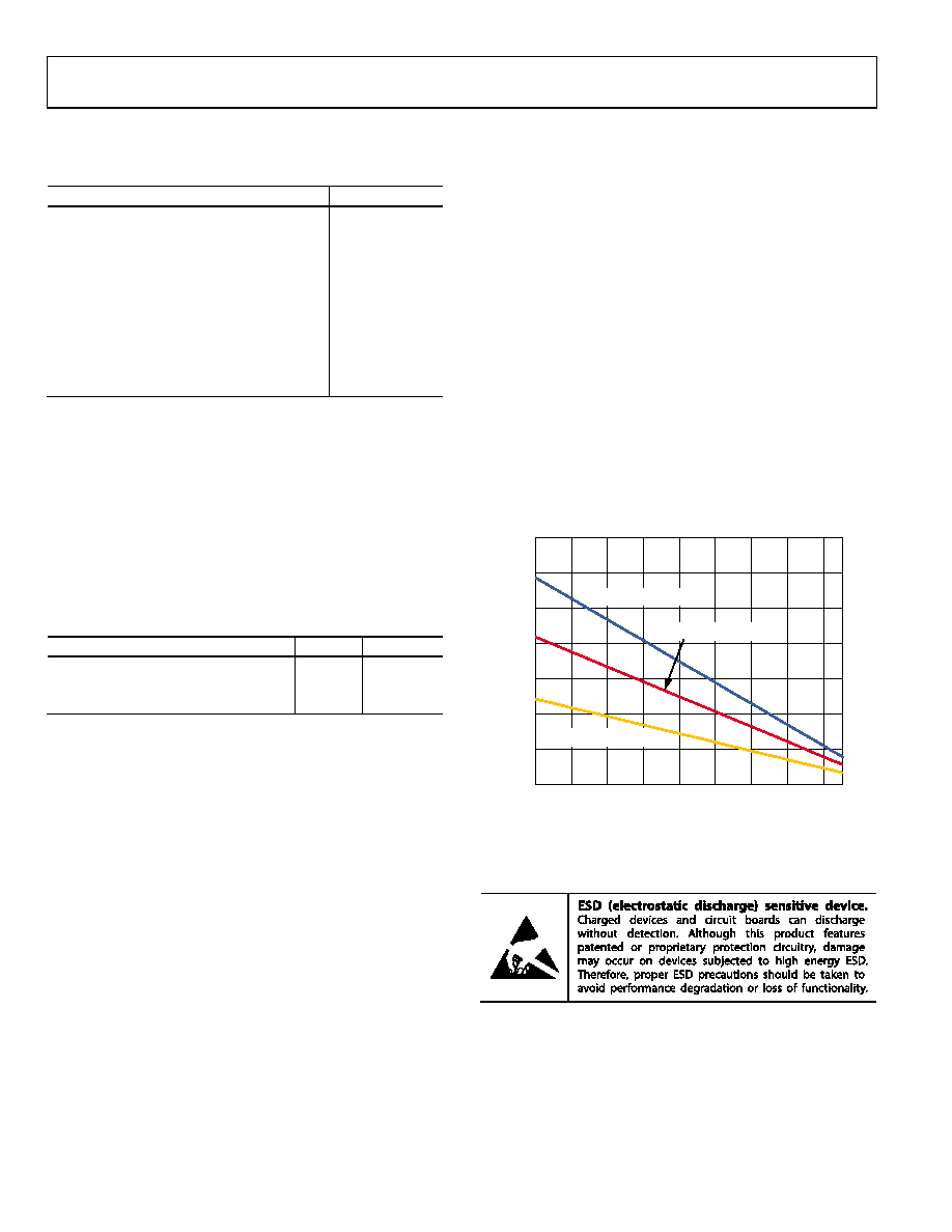
Figure 3 shows the maximum safe power dissipation in the
package vs. the ambient temperature for the 8-lead SOIC (θJA =
158°C/W, single) the 16-lead LFCSP (θJA = 91.3°C/W, single)
and 24-lead LFCSP (θJA = 65.1°C/W, dual) packages on a JEDEC
standard 4-layer board. θJA values are approximations.
3.5
0
–40
–20
0
20
40
60
120
100
80
MA
XI
MU
M
PO
W
ER
D
ISSI
PA
T
IO
N
(W
)
AMBIENT TEMPERATURE (°C)
08452-
004
0.5
1.0
1.5
2.0
2.5
3.0
ADA4940-2 (LFCSP)
ADA4940-1 (LFCSP)
ADA4940-1 (SOIC)
Figure 3. Maximum Safe Power Dissipation vs. Ambient Temperature
ESD CAUTION
相关PDF资料 |
PDF描述 |
|---|---|
| ADA4950-1YCPZ-RL | IC AMP DIFF LP 114MA 16LFCSP |
| ADEL2020ARZ-20-RL | IC OPAMP CF LN LP 60MA 20SOIC |
| ADL5561ACPZ-R7 | IC AMP DIFF RF/IF 2.9GHZ 16LFCSP |
| ADL5562ACPZ-R7 | IC AMP DIFF RF/IF 3.3GHZ 16LFCSP |
| ADL5565ACPZ-R7 | IC AMP DIFF 6GHZ 16LFCSP |
相关代理商/技术参数 |
参数描述 |
|---|---|
| ADA4940-1ARZ-RL | 功能描述:IC DIFF ADC DVR 18BIT LN 8SOIC RoHS:是 类别:集成电路 (IC) >> Linear - Amplifiers - Instrumentation 系列:- 标准包装:50 系列:- 放大器类型:通用 电路数:2 输出类型:满摆幅 转换速率:1.8 V/µs 增益带宽积:6.5MHz -3db带宽:4.5MHz 电流 - 输入偏压:5nA 电压 - 输入偏移:100µV 电流 - 电源:65µA 电流 - 输出 / 通道:35mA 电压 - 电源,单路/双路(±):1.8 V ~ 5.25 V,±0.9 V ~ 2.625 V 工作温度:-40°C ~ 85°C 安装类型:表面贴装 封装/外壳:10-TFSOP,10-MSOP(0.118",3.00mm 宽) 供应商设备封装:10-MSOP 包装:管件 |
| ADA4940-1XCPZ-R7 | 制造商:Analog Devices 功能描述: |
| ADA4940-2 | 制造商:AD 制造商全称:Analog Devices 功能描述:Ultralow Power, Low Distortion |
| ADA4940-2ACP-EBZ | 制造商:Analog Devices 功能描述:EVAL BOARD DUAL DIFFERENTIAL 制造商:Analog Devices 功能描述:ADA4940-2, DIFF AMP, EVAL BOARD |
| ADA4940-2ACPZ-R2 | 制造商:Analog Devices 功能描述:SUB 10M W ADC DRIVER FOR PULSAR FAMILY - Tape and Reel |
发布紧急采购,3分钟左右您将得到回复。