- 您现在的位置:买卖IC网 > PDF目录2139 > ADA4940-1ARZ-R7 (Analog Devices Inc)IC DIFF ADC DVR 18BIT LN 8SOIC PDF资料下载
参数资料
| 型号: | ADA4940-1ARZ-R7 |
| 厂商: | Analog Devices Inc |
| 文件页数: | 17/33页 |
| 文件大小: | 0K |
| 描述: | IC DIFF ADC DVR 18BIT LN 8SOIC |
| 标准包装: | 1,000 |
| 放大器类型: | 差分 |
| 电路数: | 1 |
| 输出类型: | 差分 |
| 转换速率: | 95 V/µs |
| -3db带宽: | 260MHz |
| 电流 - 输入偏压: | 1.1µA |
| 电压 - 输入偏移: | 60µV |
| 电流 - 电源: | 1.25mA |
| 电流 - 输出 / 通道: | 46mA |
| 电压 - 电源,单路/双路(±): | 3 V ~ 6 V |
| 工作温度: | -40°C ~ 125°C |
| 安装类型: | 表面贴装 |
| 封装/外壳: | 8-SOIC(0.154",3.90mm 宽) |
| 供应商设备封装: | 8-SO |
| 包装: | 带卷 (TR) |
第1页第2页第3页第4页第5页第6页第7页第8页第9页第10页第11页第12页第13页第14页第15页第16页当前第17页第18页第19页第20页第21页第22页第23页第24页第25页第26页第27页第28页第29页第30页第31页第32页第33页
Data Sheet
ADA4940-1/ADA4940-2
Rev. C | Page 23 of 32
APPLICATIONS INFORMATION
ANALYZING AN APPLICATION CIRCUIT
The ADA4940-1/ADA4940-2 use open-loop gain and negative
feedback to force their differential and common-mode output
voltages in such a way as to minimize the differential and common-
mode error voltages. The differential error voltage is defined as
the voltage between the differential inputs labeled +IN and IN (see
Figure 61). For most purposes, this voltage can be assumed to be
zero. Similarly, the difference between the actual output common-
mode voltage and the voltage applied to VOCM can also be assumed
to be zero. Starting from these two assumptions, any application
circuit can be analyzed.
SETTING THE CLOSED-LOOP GAIN
The differential mode gain of the circuit in Figure 61 can be
determined by
G
F
dm
IN
dm
OUT
R
V
=
,
This assumes that the input resistors (RG) and feedback resistors
(RF) on each side are equal.
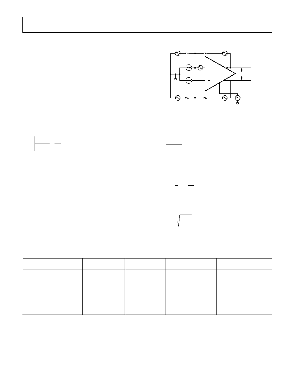
ESTIMATING THE OUTPUT NOISE VOLTAGE
The differential output noise of the ADA4940-1/ADA4940-2 can
be estimated using the noise model in Figure 63. The input-referred
noise voltage density, vnIN, is modeled as a differential input, and
the noise currents, inIN and inIN+, appear between each input and
ground. The noise currents are assumed to be equal and produce
a voltage across the parallel combination of the gain and feedback
resistances. vnCM is the noise voltage density at the VOCM pin. Each
the input noise sources, the multiplication factors, and the
output-referred noise density terms. For more noise calculation
information, go to the Analog Devices Differential Amplifier
Calculator (DiffAmpCalc), click ADIDiffAmpCalculator.zip
and follow the on-screen prompts.
ADA4940-1/
ADA4940-2
+
RF2
VnOD
VnCM
VOCM
VnIN
RF1
RG2
RG1
VnRF1
VnRF2
VnRG1
VnRG2
inIN+
inIN–
08452-
050
Figure 63. ADA4940-1/ADA4940-2 Noise Model
As with conventional op amp, the output noise voltage densities
can be estimated by multiplying the input-referred terms at +IN
and IN by the appropriate output factor,
where:
(
)
2
1
N
β
G
+
=
2
is the circuit noise gain.
G1
F1
G1
1
R
β
+
=
and
G2
F2
G2
2
R
β
+
=
are the feedback factors.
When RF1/RG1 = RF2/RG2, then β1 = β2 = β, and the noise gain
becomes
G
F
N
R
β
G
+
=
1
Note that the output noise from VOCM goes to zero in this case.
The total differential output noise density, vnOD, is the root-sum-
square of the individual output noise terms.
∑
=
8
1
i
2
nOi
nOD
v
Table 14. Output Noise Voltage Density Calculations
Input Noise Contribution
Input Noise Term
Input Noise
Voltage Density
Output
Multiplication Factor
Output-Referred Noise
Voltage Density Term
Differential Input
vnIN
GN
vnO1 = GN (vnIN)
Inverting Input
inIN
inIN × (RG2||RF2)
GN
vnO2 = GN [inIN × (RG2||RF2)]
Noninverting Input
inIN+
inIN+ × (RG1||RF1)
GN
vnO3 = GN [inIN+ × (RG1||RF1)]
VOCM Input
vnCM
GN (β1 β2)
vnO4 = GN (β1 β2)(vnCM)
Gain Resistor RG1
vnRG1
(4kTRG1)1/2
GN (1 β2)
vnO5 = GN (1 β2)(4kTRG1)1/2
Gain Resistor RG2
vnRG2
(4kTRG2)1/2
GN (1 β1)
vnO6 = GN (1 β1)(4kTRG2)1/2
Feedback Resistor RF1
vnRF1
(4kTRF1)1/2
1
vnO7 = (4kTRF1)1/2
Feedback Resistor RF2
vnRF2
(4kTRF2)1/2
1
vnO8 = (4kTRF2)1/2
相关PDF资料 |
PDF描述 |
|---|---|
| ADA4950-1YCPZ-RL | IC AMP DIFF LP 114MA 16LFCSP |
| ADEL2020ARZ-20-RL | IC OPAMP CF LN LP 60MA 20SOIC |
| ADL5561ACPZ-R7 | IC AMP DIFF RF/IF 2.9GHZ 16LFCSP |
| ADL5562ACPZ-R7 | IC AMP DIFF RF/IF 3.3GHZ 16LFCSP |
| ADL5565ACPZ-R7 | IC AMP DIFF 6GHZ 16LFCSP |
相关代理商/技术参数 |
参数描述 |
|---|---|
| ADA4940-1ARZ-RL | 功能描述:IC DIFF ADC DVR 18BIT LN 8SOIC RoHS:是 类别:集成电路 (IC) >> Linear - Amplifiers - Instrumentation 系列:- 标准包装:50 系列:- 放大器类型:通用 电路数:2 输出类型:满摆幅 转换速率:1.8 V/µs 增益带宽积:6.5MHz -3db带宽:4.5MHz 电流 - 输入偏压:5nA 电压 - 输入偏移:100µV 电流 - 电源:65µA 电流 - 输出 / 通道:35mA 电压 - 电源,单路/双路(±):1.8 V ~ 5.25 V,±0.9 V ~ 2.625 V 工作温度:-40°C ~ 85°C 安装类型:表面贴装 封装/外壳:10-TFSOP,10-MSOP(0.118",3.00mm 宽) 供应商设备封装:10-MSOP 包装:管件 |
| ADA4940-1XCPZ-R7 | 制造商:Analog Devices 功能描述: |
| ADA4940-2 | 制造商:AD 制造商全称:Analog Devices 功能描述:Ultralow Power, Low Distortion |
| ADA4940-2ACP-EBZ | 制造商:Analog Devices 功能描述:EVAL BOARD DUAL DIFFERENTIAL 制造商:Analog Devices 功能描述:ADA4940-2, DIFF AMP, EVAL BOARD |
| ADA4940-2ACPZ-R2 | 制造商:Analog Devices 功能描述:SUB 10M W ADC DRIVER FOR PULSAR FAMILY - Tape and Reel |
发布紧急采购,3分钟左右您将得到回复。