- 您现在的位置:买卖IC网 > PDF目录2063 > ADAU1401AWBSTZ-RL (Analog Devices Inc)IC AUDIO PROC 28/56BIT 48LQFP PDF资料下载
参数资料
| 型号: | ADAU1401AWBSTZ-RL |
| 厂商: | Analog Devices Inc |
| 文件页数: | 39/52页 |
| 文件大小: | 0K |
| 描述: | IC AUDIO PROC 28/56BIT 48LQFP |
| 标准包装: | 2,000 |
| 系列: | SigmaDSP® |
| 类型: | 音频处理器 |
| 应用: | 监控器,电视 |
| 安装类型: | 表面贴装 |
| 封装/外壳: | 48-LQFP |
| 供应商设备封装: | 48-LQFP(7x7) |
| 包装: | 带卷 (TR) |
第1页第2页第3页第4页第5页第6页第7页第8页第9页第10页第11页第12页第13页第14页第15页第16页第17页第18页第19页第20页第21页第22页第23页第24页第25页第26页第27页第28页第29页第30页第31页第32页第33页第34页第35页第36页第37页第38页当前第39页第40页第41页第42页第43页第44页第45页第46页第47页第48页第49页第50页第51页第52页
ADAU1401A
Rev. A | Page 44 of 52
MULTIPURPOSE PINS
The ADAU1401A has 12 multipurpose (MP) pins that can be
individually programmed to be used as serial data inputs, serial
data outputs, digital control inputs to and outputs from the
SigmaDSP core, or inputs to the 4-channel auxiliary ADC. These
pins allow the ADAU1401A to be used with external ADCs and
DACs. They also use analog or digital inputs to control settings
such as volume control or use output digital signals to drive LED
indicators. Every MP pin has an internal 15 kΩ pull-up resistor.
AUXILIARY ADC
The ADAU1401A has a 4-channel, 8-bit auxiliary ADC that can be
used in conjunction with a potentiometer to control volume, tone,
or other parameter settings in the DSP program. Each of the four
channels is sampled at the audio sampling frequency (fS). Full-scale
input on this ADC is 3.0 V, thus the step size is approximately
12 mV (3.0 V/256 steps). The input resistance of the ADC is
approximately 30 kΩ. Table 63 indicates which four MP pins are
mapped to the four channels of the auxiliary ADC. The auxiliary
ADC is enabled for those pins by writing 1111 to the appropriate
portion of the multipurpose pin configuration registers.
The auxiliary ADC is turned on by setting the AAEN bit of the
auxiliary ADC enable register (see Table 58).
Noise on the ADC input can cause the digital output to constantly
change by a few LSBs. If the auxiliary ADC is used to control
volume, this constant change causes small gain fluctuations. To
avoid this, add a low-pass filter or hysteresis to the auxiliary ADC
signal path by enabling either function in the auxiliary ADC and
power control register (Address 2082), as described in Table 56.
The filter is enabled by default when the auxiliary ADC is enabled.
When data is read from the auxiliary ADC registers, two bytes
(12 bits of data, plus zero-padded LSBs) are available because of
this filtering.
20k
10k
S1
S2
1.8pF
AUX ADC
INPUT PIN
08
506
-03
0
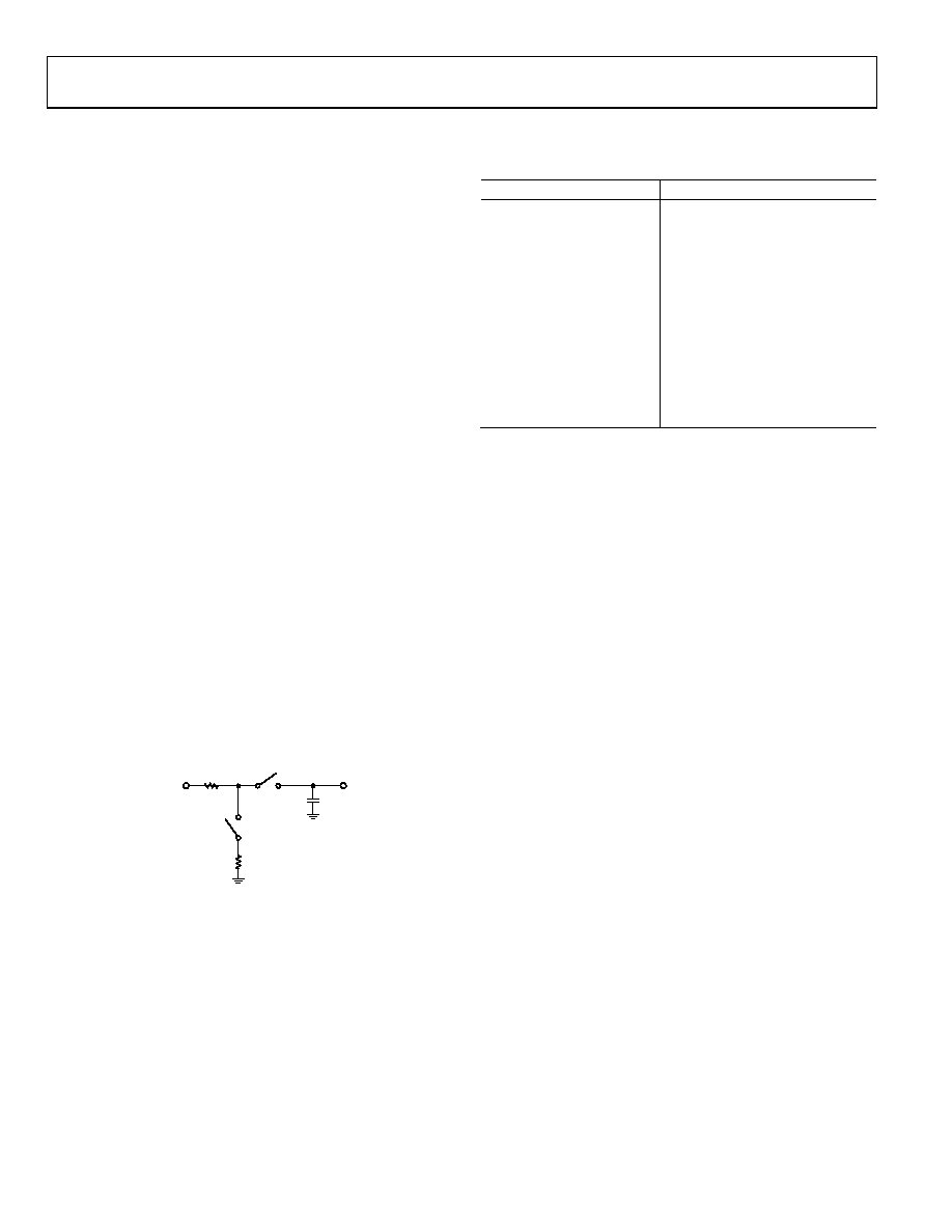
Figure 31. Auxiliary ADC Input Circuit
Figure 31 shows the input circuit for the auxiliary ADC. Switch
S1 enables the auxiliary ADC and is set by Bit 15 (AAEN) of the
auxiliary ADC enable register. The sampling switch, S2, operates at
the audio sampling frequency.
The auxiliary ADC data registers can be written to directly after
AACW has been set in the DSP core control register. In this mode,
the voltages on the analog inputs are not written into the registers,
but rather the data in the registers is written from the control port.
PVDD supplies the 3.3 V power for the auxiliary ADC analog
input. The digital core of the auxiliary ADC is powered by the
1.8 V DVDD signal.
Table 63. Multipurpose Pin Auxiliary ADC Mapping
Multipurpose Pin
Function
MP0
N/A
MP1
N/A
MP2
ADC1
MP3
ADC2
MP4
N/A
MP5
N/A
MP6
N/A
MP7
N/A
MP8
ADC3
MP9
ADC0
MP10
N/A
MP11
N/A
GENERAL-PURPOSE INPUT/OUTPUT PINS
The general-purpose input/output (GPIO) pins can be used as
inputs or outputs. These pins are readable and can be set either
through the control interface or directly by the SigmaDSP core.
When set as inputs, these pins can be used with push-button
switches or rotary encoders to control DSP program settings.
Digital outputs can be used to drive LEDs or external logic to
indicate the status of internal signals and control other devices.
Examples of this use include indicating signal overload, signal
present, and confirmation of pressing a button.
When set as an output, each pin can typically drive 2 mA. This
is enough current to directly drive some high efficiency LEDs.
Standard LEDs require about 20 mA of current and can be
driven from a GPIO output with an external transistor or buffer.
Because of issues that may arise from simultaneously driving or
sinking a large current on many pins, care should be taken in
the application design to avoid connecting high efficiency LEDs
directly to many or all of the MPx pins. If many LEDs are required,
use an external driver.
When the GPIO pins are set as open-collector outputs, they
should be pulled up to a maximum voltage of 3.3 V (the voltage
on IOVDD).
SERIAL DATA INPUT/OUTPUT PORTS
The flexible serial data input and output ports of the ADAU1401A
can be set to accept or transmit data in 2-channel format or in an
8-channel TDM stream. Data is processed in twos complement,
MSB-first format. The left-channel data field always precedes
the right-channel data field in the 2-channel streams. In TDM
mode, Slot 0 to Slot 3 are in the first half of the audio frame, and
Slot 4 to Slot 7 are in the second half of the frame. TDM mode
allows fewer multipurpose pins to be used, freeing more pins
for other functions. The serial modes are set in the serial output
and serial input control registers.
The serial data clocks must be synchronous with the ADAU1401A
master clock input. The serial input control register allows control of
相关PDF资料 |
PDF描述 |
|---|---|
| ADAU1401YSTZ-RL | IC AUDIO PROC 28/56BIT 48LQFP |
| ADAU1442YSVZ-3A-RL | IC SIGMADSP 28B 175MHZ 100TQFP |
| ADAU1445YSVZ-3A-RL | IC SIGMADSP 175MHZ 100TQFP |
| ADAU1461WBCPZ-R7 | IC SIGMADSP 24BIT 96KHZ PLL 32 |
| ADAU1513ACPZ-RL7 | IC AMP AUDIO PWR 23W 48LFCSP |
相关代理商/技术参数 |
参数描述 |
|---|---|
| ADAU1401YSTZ | 功能描述:IC AUDIO PROC 28/56BIT 48LQFP RoHS:是 类别:集成电路 (IC) >> 线性 - 音频处理 系列:SigmaDSP® 其它有关文件:STA321 View All Specifications 标准包装:1 系列:Sound Terminal™ 类型:音频处理器 应用:数字音频 安装类型:表面贴装 封装/外壳:64-LQFP 裸露焊盘 供应商设备封装:64-LQFP EP(10x10) 包装:Digi-Reel® 其它名称:497-11050-6 |
| ADAU1401YSTZ-RL | 功能描述:IC AUDIO PROC 28/56BIT 48LQFP RoHS:是 类别:集成电路 (IC) >> 线性 - 音频处理 系列:SigmaDSP® 其它有关文件:STA321 View All Specifications 标准包装:1 系列:Sound Terminal™ 类型:音频处理器 应用:数字音频 安装类型:表面贴装 封装/外壳:64-LQFP 裸露焊盘 供应商设备封装:64-LQFP EP(10x10) 包装:Digi-Reel® 其它名称:497-11050-6 |
| ADAU1421YSTZ | 制造商:Analog Devices 功能描述: |
| ADAU1421YSTZ-REEL | 制造商:Analog Devices 功能描述: |
| ADAU1442 | 制造商:AD 制造商全称:Analog Devices 功能描述:SigmaDSP Digital Audio Processor |
发布紧急采购,3分钟左右您将得到回复。