- 您现在的位置:买卖IC网 > PDF目录2063 > ADAU1401AWBSTZ-RL (Analog Devices Inc)IC AUDIO PROC 28/56BIT 48LQFP PDF资料下载
参数资料
| 型号: | ADAU1401AWBSTZ-RL |
| 厂商: | Analog Devices Inc |
| 文件页数: | 9/52页 |
| 文件大小: | 0K |
| 描述: | IC AUDIO PROC 28/56BIT 48LQFP |
| 标准包装: | 2,000 |
| 系列: | SigmaDSP® |
| 类型: | 音频处理器 |
| 应用: | 监控器,电视 |
| 安装类型: | 表面贴装 |
| 封装/外壳: | 48-LQFP |
| 供应商设备封装: | 48-LQFP(7x7) |
| 包装: | 带卷 (TR) |
第1页第2页第3页第4页第5页第6页第7页第8页当前第9页第10页第11页第12页第13页第14页第15页第16页第17页第18页第19页第20页第21页第22页第23页第24页第25页第26页第27页第28页第29页第30页第31页第32页第33页第34页第35页第36页第37页第38页第39页第40页第41页第42页第43页第44页第45页第46页第47页第48页第49页第50页第51页第52页
ADAU1401A
Rev. A | Page 17 of 52
INITIALIZATION
This section describes the procedure for properly setting up the
ADAU1401A. The following five-step sequence provides an
overview of how to initialize the IC:
1.
Apply power to the ADAU1401A.
2.
Wait for the PLL to lock.
3.
Load the SigmaDSP program and parameters.
4.
Set up registers (including multipurpose pins and digital
interfaces).
5.
Turn off the default muting of the converters, clear the
data registers, and initialize the DAC setup register (see
the Control Registers Setup section for specific settings).
To only test analog audio pass-through (ADCs to DACs), skip
Step 3 and Step 4 and use the default internal program.
POWER-UP SEQUENCE
The ADAU1401A has a built-in power-up sequence that initializes
the contents of all internal RAMs on power-up or when the device
is brought out of a reset. On the rising edge of RESET, the contents
of the internal program boot ROM are copied to the internal
program RAM memory, the parameter RAM is filled with values
(all 0s) from its associated boot ROM, and all registers are
initialized to 0s. The default boot ROM program copies audio
from the inputs to the outputs without processing it (see
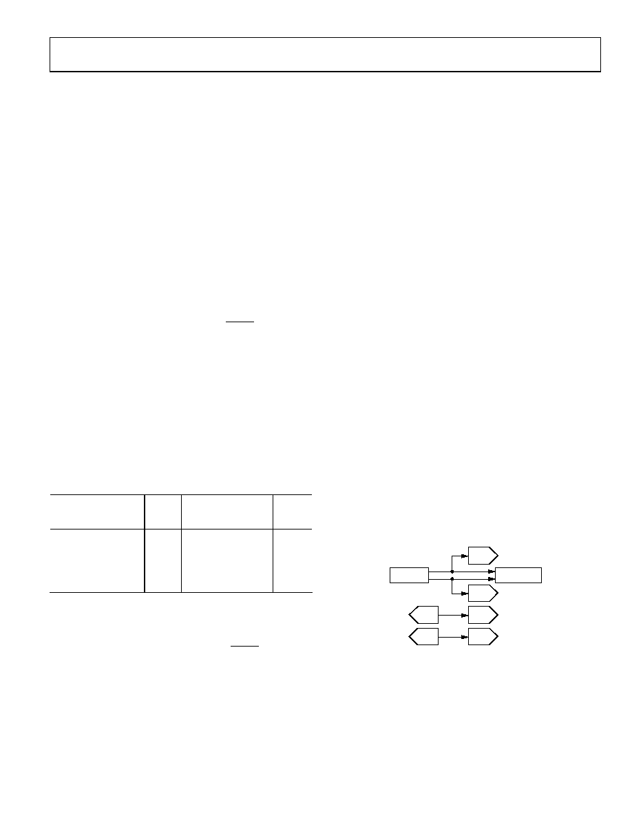
). In this program, SDATA_IN0 and SDATA_IN1 are output
on DAC0 and DAC1 and on SDATA_OUT0 and
SDATA_OUT1. ADC0 and ADC1 are output on DAC2 and
DAC3. The data memories are also zeroed at power-up. New
values should not be written to the control port until the
initialization is complete.
Table 12. Power-Up Time
MCLKI Input
Frequency
Init.
Time
Maximum Program/
Parameter/Register
Boot Time (I2C)
Total
Time
3.072 MHz (64 × fS)
85 ms
175 ms
260 ms
11.2896 MHz (256 × fS)
23 ms
175 ms
198 ms
12.288 MHz (256 × fS)
21 ms
175 ms
196 ms
18.432 MHz (384 × fS)
16 ms
175 ms
191 ms
24.576 MHz (512 × fS)
11 ms
175 ms
186 ms
The PLL start-up time lasts for 218 cycles of the clock on the
MCLKI pin. This time ranges from 10.7 ms for a 24.576 MHz
(512 × fS) input clock to 85.3 ms for a 3.072 MHz (64 × fS) input
clock and is measured from the rising edge of RESET. Following
the PLL startup, the duration of the ADAU1401A boot cycle is
about 42 μs for a fS of 48 kHz. The user should avoid writing to or
reading from the ADAU1401A during this start-up time. For an
MCLKI input signal of 12.288 MHz, the full initialization sequence
(PLL startup plus boot cycle) is approximately 21 ms. As the device
comes out of a reset, the clock mode is immediately set by the
PLL_MODE0 and PLL_MODE1 pins. The reset is synchronized
to the falling edge of the internal clock.
Table 12 lists typical times to boot the ADAU1401A into an
operational state for an application, assuming a 400 kHz I2C
clock loading a full program, parameter set, and all registers
(about 8.5 kB). In reality, most applications do not fill the RAMs
and, therefore, boot time is less than the value listed in Column 3
of Table 12.
CONTROL REGISTERS SETUP
The following registers must be set as described in this section
to initialize the ADAU1401A. These settings are the basic
minimum settings needed to operate the IC with an analog
input/output of 48 kHz. More registers may need to be set,
depending on the application. See the RAMs and Registers
section for additional settings.
DSP Core Control Register (Address 2076)
Set Bits[4:2] (ADM, DAM, and CR) each to 111.
DAC Setup Register (Address 2087)
Set Bits[1:0] (DS[1:0]) to 01.
RECOMMENDED PROGRAM/PARAMETER
LOADING PROCEDURE
When writing large amounts of data to the program or para-
meter RAM in direct write mode, the processor core should
be disabled to prevent unpleasant noises from appearing in
the audio output. To disable the processor core,
1.
Set Bits[4:3] (active low) of the DSP core control register
(Address 2076) to 1 to mute the ADCs and DACs. This
begins a volume ramp-down.
2.
Set Bit 2 (active low) of the DSP core control register to 1.
This zeroes the SigmaDSP accumulators, the data output
registers, and the data input registers.
3.
Fill the program RAM using burst mode writes.
4.
Fill the parameter RAM using burst mode writes.
5.
Set Bits[4:2] of the DSP core control register to 111.
ADC0
DAC1
DAC0
DAC2
DAC3
ADC1
SDATA_IN0
SDATA_OUT0
08
50
6-
01
3
Figure 13. Default Program Signal Flow
POWER REDUCTION MODES
Sections of the ADAU1401A chip can be turned on and off as
needed to reduce power consumption. These include the ADCs,
DACs, and voltage reference.
The individual analog sections can be turned off by writing to
the auxiliary ADC and power control register (Address 2082).
By default, the ADCs, DACs, and reference are enabled (all bits
相关PDF资料 |
PDF描述 |
|---|---|
| ADAU1401YSTZ-RL | IC AUDIO PROC 28/56BIT 48LQFP |
| ADAU1442YSVZ-3A-RL | IC SIGMADSP 28B 175MHZ 100TQFP |
| ADAU1445YSVZ-3A-RL | IC SIGMADSP 175MHZ 100TQFP |
| ADAU1461WBCPZ-R7 | IC SIGMADSP 24BIT 96KHZ PLL 32 |
| ADAU1513ACPZ-RL7 | IC AMP AUDIO PWR 23W 48LFCSP |
相关代理商/技术参数 |
参数描述 |
|---|---|
| ADAU1401YSTZ | 功能描述:IC AUDIO PROC 28/56BIT 48LQFP RoHS:是 类别:集成电路 (IC) >> 线性 - 音频处理 系列:SigmaDSP® 其它有关文件:STA321 View All Specifications 标准包装:1 系列:Sound Terminal™ 类型:音频处理器 应用:数字音频 安装类型:表面贴装 封装/外壳:64-LQFP 裸露焊盘 供应商设备封装:64-LQFP EP(10x10) 包装:Digi-Reel® 其它名称:497-11050-6 |
| ADAU1401YSTZ-RL | 功能描述:IC AUDIO PROC 28/56BIT 48LQFP RoHS:是 类别:集成电路 (IC) >> 线性 - 音频处理 系列:SigmaDSP® 其它有关文件:STA321 View All Specifications 标准包装:1 系列:Sound Terminal™ 类型:音频处理器 应用:数字音频 安装类型:表面贴装 封装/外壳:64-LQFP 裸露焊盘 供应商设备封装:64-LQFP EP(10x10) 包装:Digi-Reel® 其它名称:497-11050-6 |
| ADAU1421YSTZ | 制造商:Analog Devices 功能描述: |
| ADAU1421YSTZ-REEL | 制造商:Analog Devices 功能描述: |
| ADAU1442 | 制造商:AD 制造商全称:Analog Devices 功能描述:SigmaDSP Digital Audio Processor |
发布紧急采购,3分钟左右您将得到回复。