- 您现在的位置:买卖IC网 > PDF目录2063 > ADAU1401YSTZ-RL (Analog Devices Inc)IC AUDIO PROC 28/56BIT 48LQFP PDF资料下载
参数资料
| 型号: | ADAU1401YSTZ-RL |
| 厂商: | Analog Devices Inc |
| 文件页数: | 17/52页 |
| 文件大小: | 0K |
| 描述: | IC AUDIO PROC 28/56BIT 48LQFP |
| 标准包装: | 2,000 |
| 系列: | SigmaDSP® |
| 类型: | 音频处理器 |
| 应用: | 监控器,电视 |
| 安装类型: | 表面贴装 |
| 封装/外壳: | 48-LQFP |
| 供应商设备封装: | 48-LQFP(7x7) |
| 包装: | 带卷 (TR) |
第1页第2页第3页第4页第5页第6页第7页第8页第9页第10页第11页第12页第13页第14页第15页第16页当前第17页第18页第19页第20页第21页第22页第23页第24页第25页第26页第27页第28页第29页第30页第31页第32页第33页第34页第35页第36页第37页第38页第39页第40页第41页第42页第43页第44页第45页第46页第47页第48页第49页第50页第51页第52页

ADAU1401
Data Sheet
Rev. C | Page 24 of 52
I2C PORT
The ADAU1401 supports a 2-wire serial (I2C-compatible)
microprocessor bus driving multiple peripherals. Two pins,
serial data (SDA) and serial clock (SCL), carry information
between the ADAU1401 and the system I2C master controller.
In I2C mode, the ADAU1401 is always a slave on the bus,
meaning it cannot initiate a data transfer. Each slave device is
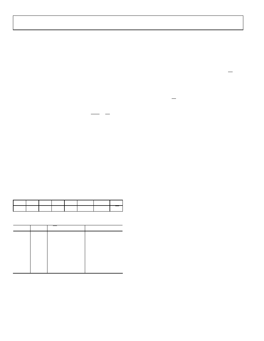
recognized by a unique address. The address byte format is
shown in Table 16. The ADAU1401 slave addresses are set with
the ADDR0 and ADDR1 pins. The address resides in the first
seven bits of the I2C write. The LSB of this byte sets either a read
or write operation. Logic Level 1 corresponds to a read operation,
and Logic Level 0 corresponds to a write operation. Bit 5 and
Bit 6 of the address are set by tying the ADDRx pins of the
ADAU1401 to Logic Level 0 or Logic Level 1. The full byte
addresses, including the pin settings and read/write (R/W) bit,
are shown in
.
Burst mode addressing, where the subaddresses are automati-
cally incremented at word boundaries, can be used for writing
large amounts of data to contiguous memory locations. This
increment happens automatically after a single-word write unless a
stop condition is encountered. The registers and RAMs in the
ADAU1401 range in width from one to five bytes, so the auto-
increment feature knows the mapping between subaddresses and
the word length of the destination register (or memory location). A
data transfer is always terminated by a stop condition.
Both SDA and SCL should have 2.2 kΩ pull-up resistors on the
lines connected to them. The voltage on these signal lines should
not be more than IOVDD (3.3 V).
Table 16. ADAU1401 I2C Address Byte Format
Bit 0
Bit 1
Bit 2
Bit 3
Bit 4
Bit 5
Bit 6
Bit 7
0
1
0
1
ADDR1
ADDR0
R/W
Table 17. ADAU1401 I2C Addresses
ADDR1
ADDR0
R/W
Slave Address
0
0x68
0
1
0x69
0
1
0
0x6A
0
1
0x6B
1
0
0x6C
1
0
1
0x6D
1
0
0x6E
1
0x6F
Addressing
Initially, each device on the I2C bus is in an idle state monitoring
the SDA and SCL lines for a start condition and the proper address.
The I2C master initiates a data transfer by establishing a start
condition, defined by a high-to-low transition on SDA while
SCL remains high. This indicates that an address/data stream
follows. All devices on the bus respond to the start condition
and shift the next eight bits (the 7-bit address plus the R/W bit)
MSB first. The device that recognizes the transmitted address
responds by pulling the data line low during the ninth clock
pulse. This ninth bit is known as an acknowledge bit. All other
devices withdraw from the bus at this point and return to the
idle condition. The R/W bit determines the direction of the
data. A Logic 0 on the LSB of the first byte means the master
writes information to the peripheral, whereas a Logic 1 means
the master reads information from the peripheral after writing
the subaddress and repeating the start address. A data transfer
takes place until a stop condition is encountered. A stop
condition occurs when SDA transitions from low to high while
SCL is held high.
shows the timing of an I2C write,
and
shows an I2C read.
Stop and start conditions can be detected at any stage during the
data transfer. If these conditions are asserted out of sequence with
normal read and write operations, the ADAU1401 immediately
jumps to the idle condition. During a given SCL high period,
the user should only issue one start condition, one stop condition,
or a single stop condition followed by a single start condition. If
an invalid subaddress is issued by the user, the ADAU1401 does
not issue an acknowledge and returns to the idle condition. If
the user exceeds the highest subaddress while in auto-increment
mode, one of two actions is taken. In read mode, the ADAU1401
outputs the highest subaddress register contents until the master
device issues a no acknowledge, indicating the end of a read. A
no-acknowledge condition is where the SDA line is not pulled
low on the ninth clock pulse on SCL. On the other hand, if the
highest subaddress location is reached while in write mode, the
data for the invalid byte is not loaded into any subaddress register,
a no acknowledge is issued by the ADAU1401, and the part returns
to the idle condition.
相关PDF资料 |
PDF描述 |
|---|---|
| ADAU1442YSVZ-3A-RL | IC SIGMADSP 28B 175MHZ 100TQFP |
| ADAU1445YSVZ-3A-RL | IC SIGMADSP 175MHZ 100TQFP |
| ADAU1461WBCPZ-R7 | IC SIGMADSP 24BIT 96KHZ PLL 32 |
| ADAU1513ACPZ-RL7 | IC AMP AUDIO PWR 23W 48LFCSP |
| ADAU1590ACPZ-RL7 | IC AMP AUDIO PWR 48LFCSP |
相关代理商/技术参数 |
参数描述 |
|---|---|
| ADAU1421YSTZ | 制造商:Analog Devices 功能描述: |
| ADAU1421YSTZ-REEL | 制造商:Analog Devices 功能描述: |
| ADAU1442 | 制造商:AD 制造商全称:Analog Devices 功能描述:SigmaDSP Digital Audio Processor |
| ADAU1442YSVZ-3A | 功能描述:IC SIGMADSP 28B 175MHZ 100TQFP RoHS:是 类别:集成电路 (IC) >> 线性 - 音频处理 系列:SigmaDSP® 其它有关文件:STA321 View All Specifications 标准包装:1 系列:Sound Terminal™ 类型:音频处理器 应用:数字音频 安装类型:表面贴装 封装/外壳:64-LQFP 裸露焊盘 供应商设备封装:64-LQFP EP(10x10) 包装:Digi-Reel® 其它名称:497-11050-6 |
| ADAU1442YSVZ-3A-RL | 功能描述:IC SIGMADSP 28B 175MHZ 100TQFP RoHS:是 类别:集成电路 (IC) >> 线性 - 音频处理 系列:SigmaDSP® 其它有关文件:STA321 View All Specifications 标准包装:1 系列:Sound Terminal™ 类型:音频处理器 应用:数字音频 安装类型:表面贴装 封装/外壳:64-LQFP 裸露焊盘 供应商设备封装:64-LQFP EP(10x10) 包装:Digi-Reel® 其它名称:497-11050-6 |
发布紧急采购,3分钟左右您将得到回复。