- 您现在的位置:买卖IC网 > PDF目录2063 > ADAU1401YSTZ-RL (Analog Devices Inc)IC AUDIO PROC 28/56BIT 48LQFP PDF资料下载
参数资料
| 型号: | ADAU1401YSTZ-RL |
| 厂商: | Analog Devices Inc |
| 文件页数: | 4/52页 |
| 文件大小: | 0K |
| 描述: | IC AUDIO PROC 28/56BIT 48LQFP |
| 标准包装: | 2,000 |
| 系列: | SigmaDSP® |
| 类型: | 音频处理器 |
| 应用: | 监控器,电视 |
| 安装类型: | 表面贴装 |
| 封装/外壳: | 48-LQFP |
| 供应商设备封装: | 48-LQFP(7x7) |
| 包装: | 带卷 (TR) |
第1页第2页第3页当前第4页第5页第6页第7页第8页第9页第10页第11页第12页第13页第14页第15页第16页第17页第18页第19页第20页第21页第22页第23页第24页第25页第26页第27页第28页第29页第30页第31页第32页第33页第34页第35页第36页第37页第38页第39页第40页第41页第42页第43页第44页第45页第46页第47页第48页第49页第50页第51页第52页
ADAU1401
Data Sheet
Rev. C | Page 12 of 52
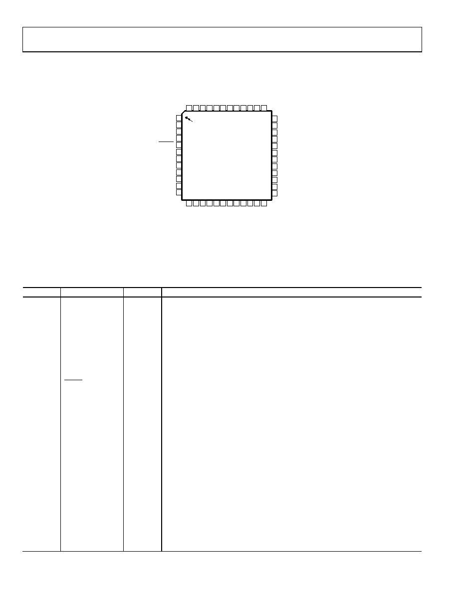
PIN CONFIGURATION AND FUNCTION DESCRIPTIONS
36
35
34
33
32
31
30
29
28
27
26
25
1
2
3
4
5
6
7
8
9
10
11
12
AVDD
PLL_LF
PVDD
PGND
MCLKI
OSCO
RSVD
MP2
MP3
MP8
MP9
DGND
DV
DD
MP
7
MP
6
MP
10
V
DRI
V
E
IOV
D
MP
11
ADDR1/
CDA
T
A/
W
B
CL
AT
C
H/
W
P
S
DA/
CO
UT
S
CL
/CCL
K
DV
DD
AGND
ADC0
ADC_RES
ADC1
RESET
SELFBOOT
ADDR0
MP4
MP5
MP1
MP0
DGND
13 14 15 16 17 18 19 20 21 22 23 24
48 47 46 45 44 43 42 41 40 39 38 37
AV
D
FIL
T
A
VO
U
T
0
VO
U
T
1
VO
U
T
2
VO
U
T
3
AG
ND
FIL
T
D
CM
PL
L
_M
O
D
E1
PL
L
_M
O
D
E0
AG
ND
ADAU1401
TOP VIEW
(Not to Scale)
PIN 1
INDICATOR
06
75
2-
0
7
Figure 7. 48-Lead LQFP Pin Configuration
Table 11. Pin Function Descriptions
Pin No.
Mnemonic
Type1
Description
1, 37, 42
AGND
PWR
Analog Ground Pin. The AGND, DGND, and PGND pins can be tied directly together in a
common ground plane. AGND should be decoupled to an AVDD pin with a 100 nF
capacitor.
2
ADC0
A_IN
Analog Audio Input 0. Full-scale 100 μA rms input. Current input allows input voltage level
to be scaled with an external resistor. An 18 kΩ resistor gives a 2 V rms full-scale input.
3
ADC_RES
A_IN
ADC Reference Current. The full-scale current of the ADCs can be set with an external 18 kΩ
resistor connected between this pin and ground. See the Audio ADCS section for details.
4
ADC1
A_IN
Analog Audio Input 1. Full-scale 100 μA rms input. Current input allows input voltage level
to be scaled with an external resistor. An 18 kΩ resistor gives a 2 V rms full-scale input. See
the Audio ADCS section for details.
5
RESET
D_IN
Active Low Reset Input. Reset is triggered on a high-to-low edge, and the ADAU1401 exits
reset on a low-to-high edge. For more information about initialization, see the Power-Up
Sequence section for details.
6
SELFBOOT
D_IN
Enable/Disable Self-Boot. SELFBOOT selects control port (low) or self-boot (high). Setting
this pin high initiates a self-boot operation when the ADAU1401 is brought out of a reset. This
pin can be tied directly to the control voltage or pulled up/down with a resistor. See the
Self-Boot section for details.
7
ADDR0
D_IN
I2C and SPI Address 0. In combination with ADDR1, this pin allows up to four ADAU1401s
to be used on the same I2C bus and up to two ICs to be used with a common SPI CLATCH
signal. See the I2C Port section for details.
8
MP4
D_IO
Multipurpose GPIO or Serial Input Port LRCLK (INPUT_LRCLK). See the Multipurpose Pins
section for more details.
9
MP5
D_IO
Multipurpose GPIO or Serial Input Port BCLK (INPUT_BCLK). See the Multipurpose Pins
section for more details.
10
MP1
D_IO
Multipurpose GPIO or Serial Input Port Data 1 (SDATA_IN0). See the Multipurpose Pins
section for more details.
11
MP0
D_IO
Multipurpose GPIO or Serial Input Port Data 0 (SDATA_IN1). See the Multipurpose Pins
section for more details.
12, 25
DGND
PWR
Digital Ground Pin. The AGND, DGND, and PGND pins can be tied directly together in a
common ground plane. DGND should be decoupled to a DVDD pin with a 100 nF
capacitor.
相关PDF资料 |
PDF描述 |
|---|---|
| ADAU1442YSVZ-3A-RL | IC SIGMADSP 28B 175MHZ 100TQFP |
| ADAU1445YSVZ-3A-RL | IC SIGMADSP 175MHZ 100TQFP |
| ADAU1461WBCPZ-R7 | IC SIGMADSP 24BIT 96KHZ PLL 32 |
| ADAU1513ACPZ-RL7 | IC AMP AUDIO PWR 23W 48LFCSP |
| ADAU1590ACPZ-RL7 | IC AMP AUDIO PWR 48LFCSP |
相关代理商/技术参数 |
参数描述 |
|---|---|
| ADAU1421YSTZ | 制造商:Analog Devices 功能描述: |
| ADAU1421YSTZ-REEL | 制造商:Analog Devices 功能描述: |
| ADAU1442 | 制造商:AD 制造商全称:Analog Devices 功能描述:SigmaDSP Digital Audio Processor |
| ADAU1442YSVZ-3A | 功能描述:IC SIGMADSP 28B 175MHZ 100TQFP RoHS:是 类别:集成电路 (IC) >> 线性 - 音频处理 系列:SigmaDSP® 其它有关文件:STA321 View All Specifications 标准包装:1 系列:Sound Terminal™ 类型:音频处理器 应用:数字音频 安装类型:表面贴装 封装/外壳:64-LQFP 裸露焊盘 供应商设备封装:64-LQFP EP(10x10) 包装:Digi-Reel® 其它名称:497-11050-6 |
| ADAU1442YSVZ-3A-RL | 功能描述:IC SIGMADSP 28B 175MHZ 100TQFP RoHS:是 类别:集成电路 (IC) >> 线性 - 音频处理 系列:SigmaDSP® 其它有关文件:STA321 View All Specifications 标准包装:1 系列:Sound Terminal™ 类型:音频处理器 应用:数字音频 安装类型:表面贴装 封装/外壳:64-LQFP 裸露焊盘 供应商设备封装:64-LQFP EP(10x10) 包装:Digi-Reel® 其它名称:497-11050-6 |
发布紧急采购,3分钟左右您将得到回复。