- 您现在的位置:买卖IC网 > PDF目录16538 > ADCLK846/PCBZ (Analog Devices Inc)BOARD EVALUATION FOR ADCLK846 PDF资料下载
参数资料
| 型号: | ADCLK846/PCBZ |
| 厂商: | Analog Devices Inc |
| 文件页数: | 3/16页 |
| 文件大小: | 0K |
| 描述: | BOARD EVALUATION FOR ADCLK846 |
| 设计资源: | Synchronizing Multiple AD9910 1 GSPS Direct Digital Synthesizers (CN0121) |
| 标准包装: | 1 |
| 主要目的: | 计时,时钟缓冲器 / 驱动器 / 接收器 / 变换器 |
| 已用 IC / 零件: | ADCLK846 |
| 主要属性: | 6 LVDS/12 CMOS 输出 |
| 次要属性: | CMOS,LVDS 输出 |
| 已供物品: | 板 |
ADCLK846
Rev. B | Page 11 of 16
FUNCTIONAL DESCRIPTION
The ADCLK846 clock input is distributed to all output channels.
Each channel bank is pin programmable for either LVDS or
CMOS levels. This allows the selection of multiple logic
configurations ranging from 6 LVDS to 12 CMOS outputs,
along with other combinations using both types of logic.
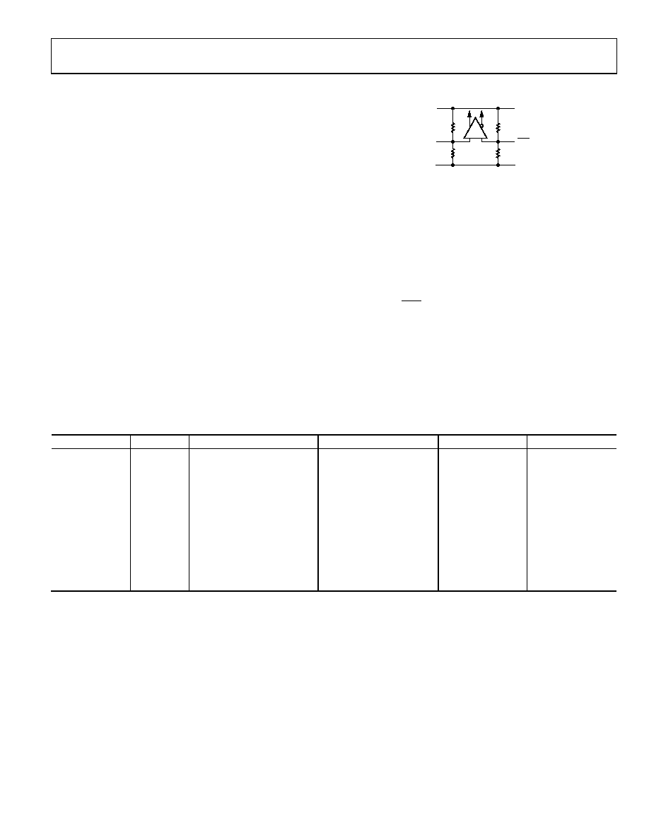
CLOCK INPUTS
The differential inputs of the ADCLK846 are internally self-
biased. The clock inputs have a resistor divider, which sets the
common-mode level for the inputs. The complementary inputs
are biased about 30 mV lower than the true input to avoid
oscillations if the input signal ceases. See Figure 20 for
the equivalent input circuit.
The inputs can be ac-coupled or dc-coupled. Table 8 displays
a guide for input logic compatibility. If a single-ended input is
desired, this can be accommodated by ac or dc coupling to one
side of the differential input. Bypass the other input to ground
by a capacitor.
Note that jitter performance degrades with low input slew rate,
different termination schemes.
9k
9.5k
9k
8.5k
VS
CLK
GND
07
22
6-
0
23
Figure 20. ADCLK846 Input Stage
AC-COUPLED APPLICATIONS
When ac coupling is desired, the ADCLK846 offers two
options. The first option requires no external components
(excluding the dc blocking capacitor); it allows the user to
couple the reference signal onto the clock input pins (see
The second option allows the use of the VREF pin to set the dc
bias level for the ADCLK846. The VREF pin can be connected
to CLK and CLK through resistors. This method allows lower
impedance termination of signals at the ADCLK846 (see
The internal bias resistors are still in parallel with the external
biasing. However, the relatively high impedance of the internal
resistors allows the external termination to VREF to dominate.
This is also useful if it is not desirable to offset the inputs slightly
as previously mentioned using only the internal biasing.
Table 8. Input Logic Compatibility
Supply (V)
Logic
Common Mode (V)
Output Swing (V)
AC-Coupled
DC-Coupled
3.3
CML
2.9
0.8
Yes
Not allowed
2.5
CML
2.1
0.8
Yes
Not allowed
1.8
CML
1.4
0.8
Yes
3.3
CMOS
1.65
3.3
Not allowed
2.5
CMOS
1.25
2.5
Not allowed
1.8
CMOS
0.9
1.8
Yes
1.5
HSTL
0.75
Yes
LVDS
1.25
0.4
Yes
3.3
LVPECL
2.0
0.8
Yes
Not allowed
2.5
LVPECL
1.2
0.8
Yes
1.8
LVPECL
0.5
0.8
Yes
相关PDF资料 |
PDF描述 |
|---|---|
| GBA24DTMT | CONN EDGECARD 48POS R/A .125 SLD |
| DC1562A-L | BOARD EVAL LTC6994-2 |
| H8PPS-4036G | DIP CABLE - HDP40S/AE40G/HDP40S |
| GEA35DTMN | CONN EDGECARD 70POS R/A .125 SLD |
| VE-J01-EZ-S | CONVERTER MOD DC/DC 12V 25W |
相关代理商/技术参数 |
参数描述 |
|---|---|
| ADCLK854 | 制造商:AD 制造商全称:Analog Devices 功能描述:1.8 V, 12-LVDS/24-CMOS Output, Low Power Clock Fanout Buffer |
| ADCLK854/PCBZ | 功能描述:BOARD EVALUATION FOR ADCLK845 RoHS:是 类别:编程器,开发系统 >> 评估演示板和套件 系列:- 标准包装:1 系列:PSoC® 主要目的:电源管理,热管理 嵌入式:- 已用 IC / 零件:- 主要属性:- 次要属性:- 已供物品:板,CD,电源 |
| ADCLK854BCPZ | 功能描述:IC CLOCK BUFFER MUX 2:12 48LFCSP RoHS:是 类别:集成电路 (IC) >> 时钟/计时 - 时钟缓冲器,驱动器 系列:- 产品培训模块:High Bandwidth Product Overview 标准包装:1,000 系列:Precision Edge® 类型:扇出缓冲器(分配) 电路数:1 比率 - 输入:输出:1:4 差分 - 输入:输出:是/是 输入:CML,LVDS,LVPECL 输出:CML 频率 - 最大:2.5GHz 电源电压:2.375 V ~ 2.625 V 工作温度:-40°C ~ 85°C 安装类型:表面贴装 封装/外壳:16-VFQFN 裸露焊盘,16-MLF? 供应商设备封装:16-MLF?(3x3) 包装:带卷 (TR) |
| ADCLK854BCPZ-REEL7 | 功能描述:IC CLOCK BUFFER MUX 2:12 48LFCSP RoHS:是 类别:集成电路 (IC) >> 时钟/计时 - 时钟缓冲器,驱动器 系列:- 标准包装:74 系列:- 类型:扇出缓冲器(分配) 电路数:1 比率 - 输入:输出:1:10 差分 - 输入:输出:是/是 输入:HCSL, LVCMOS, LVDS, LVPECL, LVTTL 输出:HCSL,LVDS 频率 - 最大:400MHz 电源电压:3 V ~ 3.6 V 工作温度:-40°C ~ 85°C 安装类型:表面贴装 封装/外壳:32-VFQFN 裸露焊盘 供应商设备封装:32-QFN(5x5) 包装:管件 |
| ADCLK905 | 制造商:AD 制造商全称:Analog Devices 功能描述:Ultrafast SiGe ECL Clock/Data Buffers |
发布紧急采购,3分钟左右您将得到回复。