- 您现在的位置:买卖IC网 > PDF目录16538 > ADCLK846/PCBZ (Analog Devices Inc)BOARD EVALUATION FOR ADCLK846 PDF资料下载
参数资料
| 型号: | ADCLK846/PCBZ |
| 厂商: | Analog Devices Inc |
| 文件页数: | 4/16页 |
| 文件大小: | 0K |
| 描述: | BOARD EVALUATION FOR ADCLK846 |
| 设计资源: | Synchronizing Multiple AD9910 1 GSPS Direct Digital Synthesizers (CN0121) |
| 标准包装: | 1 |
| 主要目的: | 计时,时钟缓冲器 / 驱动器 / 接收器 / 变换器 |
| 已用 IC / 零件: | ADCLK846 |
| 主要属性: | 6 LVDS/12 CMOS 输出 |
| 次要属性: | CMOS,LVDS 输出 |
| 已供物品: | 板 |
ADCLK846
Rev. B | Page 12 of 16
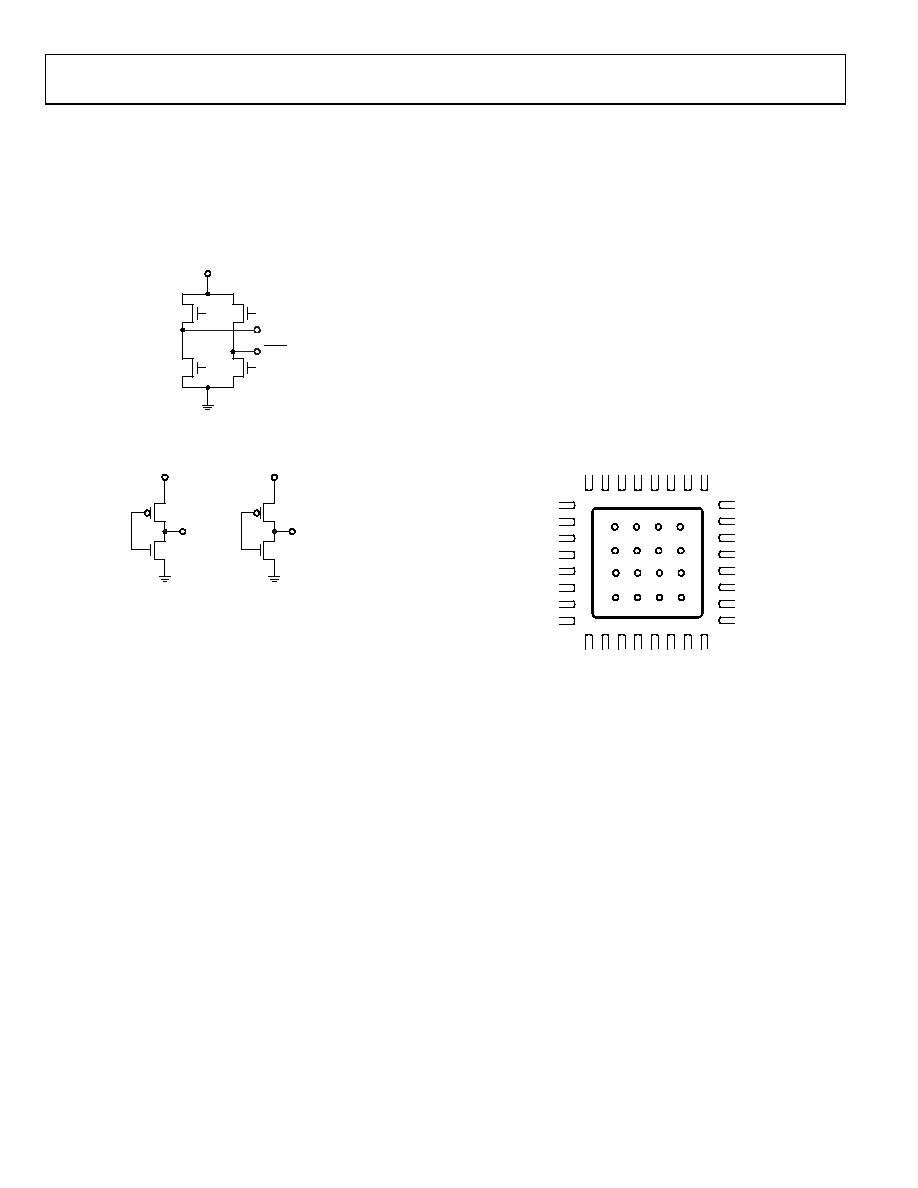
CLOCK OUTPUTS
Each driver consists of a differential LVDS output or two single-
ended CMOS outputs (always in phase). When the LVDS driver
is enabled, the corresponding CMOS driver is in tristate. When
the CMOS driver is enabled, the corresponding LVDS driver is
the equivalent output stage.
OUTx
3.5mA
VS
3.5mA
07
22
6-
024
Figure 21. LVDS Output Simplified Equivalent Circuit
OUTxA
VS
OUTxB
VS
072
26
-02
5
Figure 22. CMOS Equivalent Output Circuit
CONTROL AND FUNCTION PINS
Logic Select for CTRL_A
CTRL_A selects either CMOS (high) or LVDS (low) logic for
Output 1 and Output 0. This pin has an internal 200 kΩ pull-
down resistor.
Logic Select for CTRL_B
CTRL_B selects either CMOS (high) or LVDS (low) logic for
Output 5, Output 4, Output 3, and Output 2. This pin has an
internal 200 kΩ pull-down resistor.
Sleep Mode
SLEEP powers down the chip except for the band gap. The
input is active high, which puts the outputs into a high-Z state.
This pin has a 200 kΩ pull-down resistor. The control pins are
operational during sleep mode.
POWER SUPPLY
The ADCLK846 requires a 1.8 V ± 5% power supply for VS.
Best practice recommends bypassing the power supply on
the PCB with adequate capacitance (>10 μF) and bypassing
all power pins with adequate capacitance (0.1 μF) as close to
the part as possible. The layout of the ADCLK846 evaluation
board (ADCLK846/PCBZ) provides a good layout example.
Exposed Metal Paddle
The exposed metal paddle on the ADCLK846 package is an
electrical connection, as well as a thermal enhancement. For
the device to function properly, the paddle must be properly
attached to ground (GND). The ADCLK846 dissipates heat
through its exposed paddle. The PCB acts as a heat sink for the
ADCLK846. The PCB attachment must provide a good thermal
path to a larger heat dissipation area, such as the ground plane
on the PCB. This requires a grid of vias from the top layer down
to the ground plane. See Figure 23 for an example.
VIAS TO GND PLANE
07
22
6-
026
Figure 23. PCB Land Example for Attaching Exposed Paddle
相关PDF资料 |
PDF描述 |
|---|---|
| GBA24DTMT | CONN EDGECARD 48POS R/A .125 SLD |
| DC1562A-L | BOARD EVAL LTC6994-2 |
| H8PPS-4036G | DIP CABLE - HDP40S/AE40G/HDP40S |
| GEA35DTMN | CONN EDGECARD 70POS R/A .125 SLD |
| VE-J01-EZ-S | CONVERTER MOD DC/DC 12V 25W |
相关代理商/技术参数 |
参数描述 |
|---|---|
| ADCLK854 | 制造商:AD 制造商全称:Analog Devices 功能描述:1.8 V, 12-LVDS/24-CMOS Output, Low Power Clock Fanout Buffer |
| ADCLK854/PCBZ | 功能描述:BOARD EVALUATION FOR ADCLK845 RoHS:是 类别:编程器,开发系统 >> 评估演示板和套件 系列:- 标准包装:1 系列:PSoC® 主要目的:电源管理,热管理 嵌入式:- 已用 IC / 零件:- 主要属性:- 次要属性:- 已供物品:板,CD,电源 |
| ADCLK854BCPZ | 功能描述:IC CLOCK BUFFER MUX 2:12 48LFCSP RoHS:是 类别:集成电路 (IC) >> 时钟/计时 - 时钟缓冲器,驱动器 系列:- 产品培训模块:High Bandwidth Product Overview 标准包装:1,000 系列:Precision Edge® 类型:扇出缓冲器(分配) 电路数:1 比率 - 输入:输出:1:4 差分 - 输入:输出:是/是 输入:CML,LVDS,LVPECL 输出:CML 频率 - 最大:2.5GHz 电源电压:2.375 V ~ 2.625 V 工作温度:-40°C ~ 85°C 安装类型:表面贴装 封装/外壳:16-VFQFN 裸露焊盘,16-MLF? 供应商设备封装:16-MLF?(3x3) 包装:带卷 (TR) |
| ADCLK854BCPZ-REEL7 | 功能描述:IC CLOCK BUFFER MUX 2:12 48LFCSP RoHS:是 类别:集成电路 (IC) >> 时钟/计时 - 时钟缓冲器,驱动器 系列:- 标准包装:74 系列:- 类型:扇出缓冲器(分配) 电路数:1 比率 - 输入:输出:1:10 差分 - 输入:输出:是/是 输入:HCSL, LVCMOS, LVDS, LVPECL, LVTTL 输出:HCSL,LVDS 频率 - 最大:400MHz 电源电压:3 V ~ 3.6 V 工作温度:-40°C ~ 85°C 安装类型:表面贴装 封装/外壳:32-VFQFN 裸露焊盘 供应商设备封装:32-QFN(5x5) 包装:管件 |
| ADCLK905 | 制造商:AD 制造商全称:Analog Devices 功能描述:Ultrafast SiGe ECL Clock/Data Buffers |
发布紧急采购,3分钟左右您将得到回复。