- 您现在的位置:买卖IC网 > PDF目录10735 > ADCMP572BCPZ-WP (Analog Devices Inc)IC COMPARATOR CML 3.3-5V 16LFCSP PDF资料下载
参数资料
| 型号: | ADCMP572BCPZ-WP |
| 厂商: | Analog Devices Inc |
| 文件页数: | 16/16页 |
| 文件大小: | 0K |
| 描述: | IC COMPARATOR CML 3.3-5V 16LFCSP |
| 标准包装: | 50 |
| 类型: | 带锁销 |
| 元件数: | 1 |
| 输出类型: | CML,补充型 |
| 电压 - 电源,单路/双路(±): | 3.1 V ~ 5.4 V |
| 电压 - 输入偏移(最小值): | 2mV @ 3.3V |
| 电流 - 输入偏压(最小值): | 25µA @ 3.3V |
| 电流 - 输出(标准): | 20mA |
| 电流 - 静态(最大值): | 52mA |
| CMRR, PSRR(标准): | 65dB CMRR,74dB PSRR |
| 传输延迟(最大): | 0.165ns |
| 磁滞: | ±1mV |
| 工作温度: | -40°C ~ 85°C |
| 封装/外壳: | 16-VFQFN 裸露焊盘,CSP |
| 安装类型: | 表面贴装 |
| 包装: | 托盘 - 晶粒 |
| 配用: | EVAL-ADCMP572BCPZ-ND - BOARD EVALUATION ADCMP572BCP |
ADCMP572/ADCMP573
Rev. A | Page 9 of 16
APPLICATION INFORMATION
POWER/GROUND LAYOUT AND BYPASSING
The ADCMP572/ADCMP573 comparators are very high speed
SiGe devices. Consequently, it is essential to use proper high
speed design techniques to achieve the specified performance.
Of critical importance is the use of low impedance supply
planes, particularly the output supply plane (VCCO) and the
ground plane (GND). Individual supply planes are recom-
mended as part of a multilayer board. Providing the lowest
inductance return path for switching currents ensures the best
possible performance in the target application.
It is important to adequately bypass the input and output
supplies. A 1 μF electrolytic bypass capacitor should be placed
within several inches of each power supply pin to ground. In
addition, multiple high quality 0.01 μF bypass capacitors should
be placed as close as possible to each of the VCCI and VCCO
supply pins and should be connected to the GND plane with
redundant vias. High frequency bypass capacitors should be
carefully selected for minimum inductance and ESR. Parasitic
layout inductance should be avoided to maximize the
effectiveness of the bypass at high frequencies.
If the input and output supplies are connected separately such
that VCCI ≠ VCCO, care should be taken to bypass each of these
supplies separately to the GND plane. A bypass capacitor
should not be connected between them. It is recommended that
the GND plane separate the VCCI and VCCO planes when the
circuit board layout is designed to minimize coupling between
the two supplies and to take advantage of the additional bypass
capacitance from each respective supply to the ground plane.
This enhances the performance when split input/output
supplies are used. If the input and output supplies are connected
together for single-supply operation such that VCCI = VCCO,
coupling between the two supplies is unavoidable; however,
every effort should be made to keep the supply plane adjacent
to the GND plane to maximize the additional bypass
capacitance this arrangement provides.
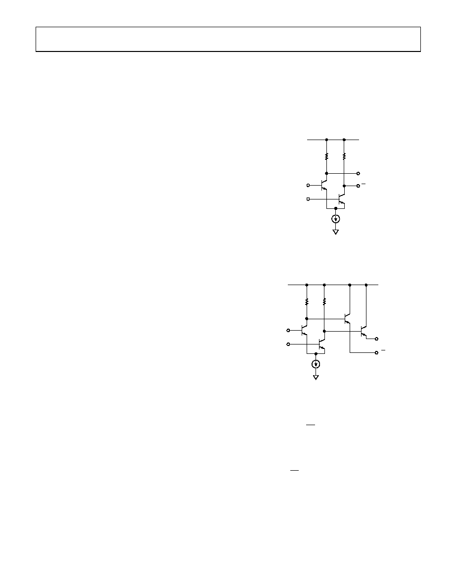
CML/RSPECL OUTPUT STAGE
Specified propagation delay dispersion performance can be
achieved only by using proper transmission line terminations.
The outputs of the ADCMP572 are designed to directly drive
400 mV into 50 Ω cable, microstrip, or strip line transmission
lines properly terminated to the VCCO supply plane. The CML
output stage is shown in the simplified schematic diagram of
Figure 15. The outputs are each back terminated with 50 Ω for
best transmission line matching. The RSPECL outputs of the
ADCMP573 are illustrated in Figure 16 and should be
terminated to VCCO 2 V. As an alternative, Thevenin
equivalent termination networks can be used in either case if
the direct termination voltage is not readily available. If high
speed output signals must be routed more than a centimeter,
microstrip or strip line techniques are essential to ensure proper
transition times and to prevent output ringing and pulse width
dependent propagation delay dispersion. For the most timing
critical applications where transmission line reflections pose the
greatest risk to performance, the ADCMP572 provides the best
match to 50 Ω output transmission paths.
Q
16mA
50
Ω
Q
04409-037
VCCO
GND
Figure 15. Simplified Schematic Diagram of
the ADCMP572 CML Output Stage
04409-038
VCCO
GND
Q
Figure 16. Simplified Schematic Diagram of
the ADCMP573 RSPECL Output Stage
USING/DISABLING THE LATCH FEATURE
The latch inputs (LE/LE) are active low for latch mode and are
internally terminated with 50 Ω resistors to Pin 8. This pin
corresponds to and is internally connected to the VCCO supply
for the CML-compatible ADCMP572. With the aid of these
resistors the ADCMP572 latch function can be disabled by
connecting the LE pin to GND with an external pull-down
resistor and leaving the LE pin unconnected. To avoid excessive
power dissipation, the resistor should be 750 Ω when VCCO =
3.3 V, and 1.2 kΩ when VCCO = 5.2 V. In the PECL-compatible
ADCMP573, the VTT pin should be connected externally to the
PECL termination supply at VCCO – 2 V. The latch can then be
disabled by connecting the LE pin to VCCO with an external
相关PDF资料 |
PDF描述 |
|---|---|
| VE-J4V-MY-F4 | CONVERTER MOD DC/DC 5.8V 50W |
| VI-JNW-MY-F2 | CONVERTER MOD DC/DC 5.5V 50W |
| VE-2WN-MY-B1 | CONVERTER MOD DC/DC 18.5V 50W |
| VE-2N4-CV-B1 | CONVERTER MOD DC/DC 48V 150W |
| VE-2WM-MY-B1 | CONVERTER MOD DC/DC 10V 50W |
相关代理商/技术参数 |
参数描述 |
|---|---|
| ADCMP572XCP | 制造商:Analog Devices 功能描述:CML ULTRAFAST 3.3V SINGLE SUPPLY COMPARATOR - Bulk |
| ADCMP573 | 制造商:AD 制造商全称:Analog Devices 功能描述:Ultrafast 3.3 V Single-Supply Comparators |
| ADCMP573BCP | 制造商:Analog Devices 功能描述:COMPARATOR SGL 5.4V 16LFCSP EP - Bulk |
| ADCMP573BCP-R2 | 制造商:Rochester Electronics LLC 功能描述: 制造商:Analog Devices 功能描述: |
| ADCMP573BCPRL7 | 制造商:AD 功能描述:NEW |
发布紧急采购,3分钟左右您将得到回复。